The cause of the potential barrier in a P−N diode is
Depletion of positive charges near the junction
Concentration of positive charges near the junction
Depletion of negative charges near the junction
Concentration of positive and negative charges near the junction
The correct Answer is:D
Step by step video, text & image solution for The cause of the potential barrier in a P-N diode is by Physics experts to help you in doubts & scoring excellent marks in Class 12 exams.
Topper's Solved these Questions
- BOOK - ERRORLESSCHAPTER - ELECTRONICSEXERCISE - Assertion & Reason26videos
ELECTRONICS
- BOOK - ERRORLESSCHAPTER - ELECTRONICSEXERCISE - NCERT Based Questions (Digital Electronics)23videos
ELECTRONICS
- BOOK - ERRORLESSCHAPTER - ELECTRON, PHOTON, PHOTOELECTRIC EFFECT & X -RAYEXERCISE - ASSERTION & REASON27videos
ELECTRON, PHOTON, PHOTOELECTRIC EFFECT & X -RAY
- BOOK - ERRORLESSCHAPTER - ELECTROSTATICSEXERCISE - ASSERTION & REASON25videos
ELECTROSTATICS
Similar Questions
The height of potential barrier in p-n junction diode is.............to temperature in kelvin.
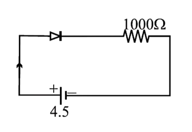
View SolutionA P-N junction diode connected to a battery of e.m.f. 4.5 V and an external resistance of 1000Ω. What is the value of current in the circuit, if potential barrier in the diode =0.5V
 View Solution
Knowledge Check
- Question 1 - Select One
In forward bias, the width of potential barrier in a P−N junction diode
AIncreasedBDecreasedCRemains constantDFirst increases and then decreases - Question 2 - Select One
In forward bias, the width of potential barrier in a P−N junction diode
ARemains constantBDecreasesCIncreasesDFirst (1) then(2) - Question 3 - Select One
In a forward biased PN- junction diode, the potential barrier in the depletion region is of the from...
A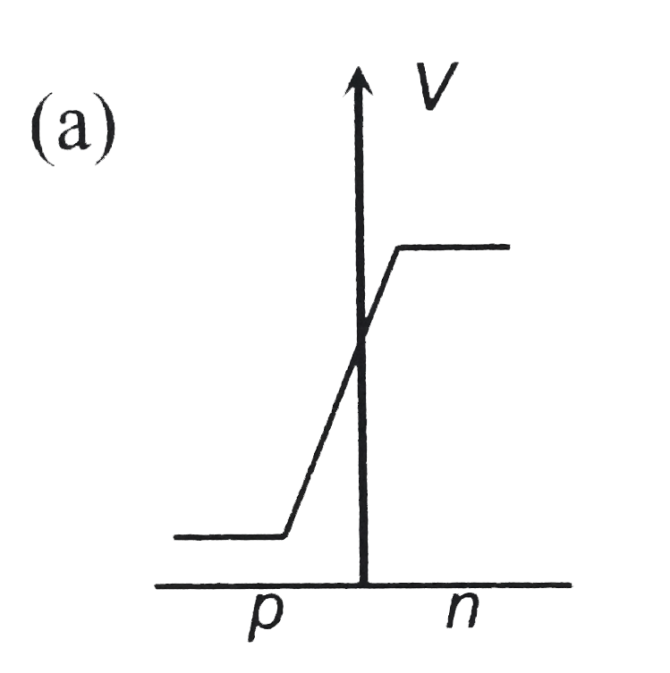 B
B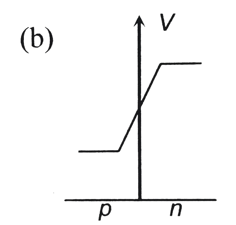 C
C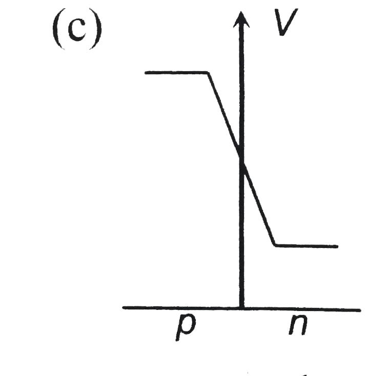 D
D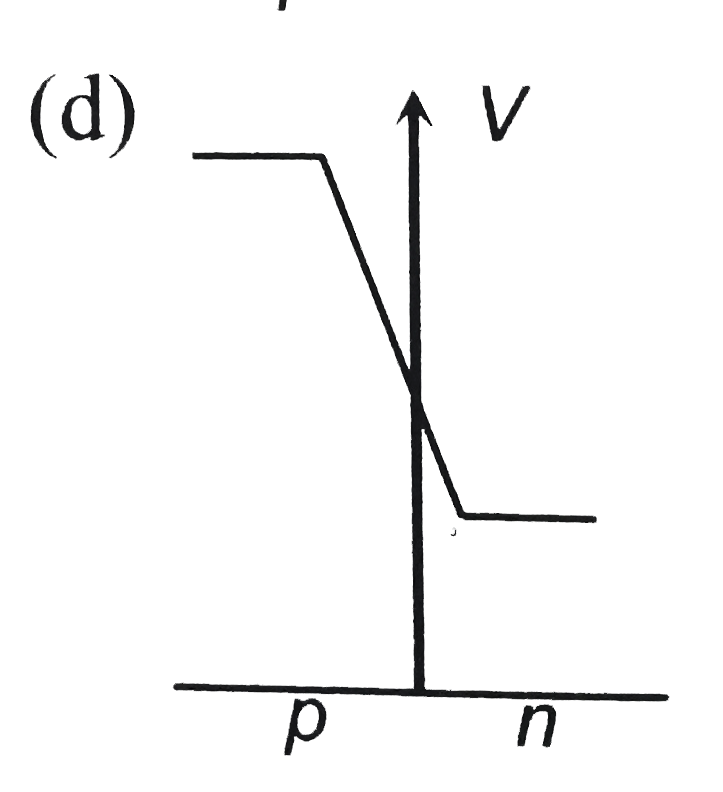
Explain the terms 'depletion layer' and 'potential barrier' in a p-n junction diode. How are the (a) width of depletion layer, and (b) value of potential barrier affected when the p-n junction is forward biased ?
View SolutionBarrier potential .
View SolutionIn a forward biased p-n junction diode, the potential barrier in the depletion region will be of the form
View SolutionThe potential barrier developed in the diode of figure is 0.5V. The current in the diode is current in the diode is
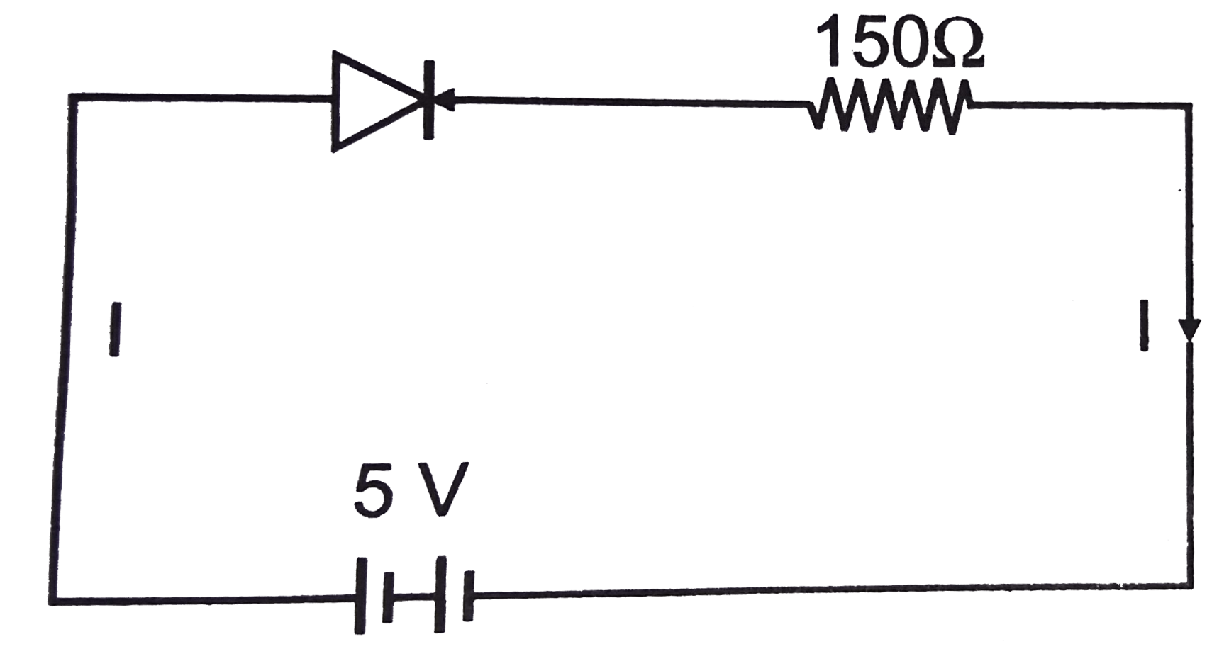 View Solution
Consider the following statements A and B and identify the correct answer.
(A)A zener diode should be connected in reverse bias for proper functioning
(B) The potential barrier of a p-n junction lies between 2 V and 5 VView Solution

