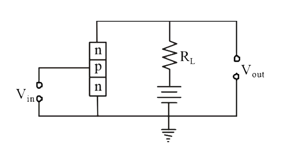
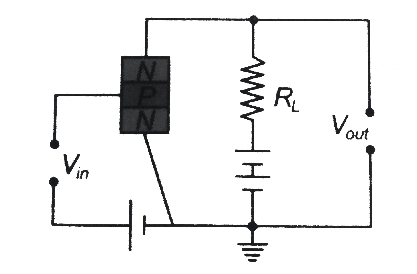
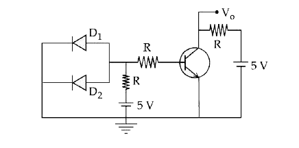
An NPN-transistor circuit is arranged as shown in figure. It is
A
Base amplifier circuit
B
Emitter amplifier circuit
C
Collector amplifier circuit
D
none of these
Video Solution
Text Solution
The correct Answer is:B
|
Answer
Step by step video & image solution for An NPN-transistor circuit is arranged as shown in figure. It is by Physics experts to help you in doubts & scoring excellent marks in Class 12 exams.
Updated on:21/07/2023Topper's Solved these Questions
- SEMICONDUCTOR ELECTRONICS: MATERIALS, DEVICES AND SIMPLE CIRCUITSBOOK - AAKASH INSTITUTECHAPTER - SEMICONDUCTOR ELECTRONICS: MATERIALS, DEVICES AND SIMPLE CIRCUITSEXERCISE - Assignment (Section -B (Objective type question (one option is correct))
29 Videos
- SEMICONDUCTOR ELECTRONICS: MATERIALS, DEVICES AND SIMPLE CIRCUITSBOOK - AAKASH INSTITUTECHAPTER - SEMICONDUCTOR ELECTRONICS: MATERIALS, DEVICES AND SIMPLE CIRCUITSEXERCISE - Assignment (Section -C(Linked comprehension type question))
3 Videos
- SEMICONDUCTOR ELECTRONICS: MATERIALS, DEVICES AND SIMPLE CIRCUITSBOOK - AAKASH INSTITUTECHAPTER - SEMICONDUCTOR ELECTRONICS: MATERIALS, DEVICES AND SIMPLE CIRCUITSEXERCISE - Try yourself
20 Videos
- SEMICONDUCTOR ELECTRONICS (MATERIAL, DEVICES AND SIMPLE CIRUITS )BOOK - AAKASH INSTITUTECHAPTER - SEMICONDUCTOR ELECTRONICS (MATERIAL, DEVICES AND SIMPLE CIRUITS )EXERCISE - Assignment SECTION - D (Assertion & reason type Question)
10 Videos
- SYSTEM OF PARTICLES AND ROTATIONAL MOTIONBOOK - AAKASH INSTITUTECHAPTER - SYSTEM OF PARTICLES AND ROTATIONAL MOTIONEXERCISE - Try Yourself
63 Videos
Similar Questions
Knowledge Check
The arrangement as shown in figure is called as
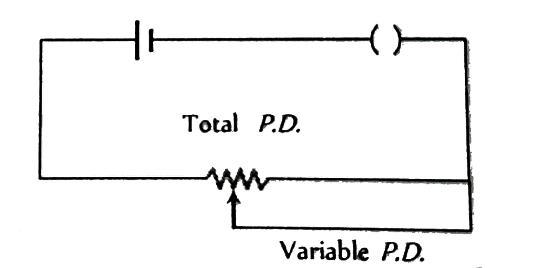 APotential dividerBPotential adderCPotential substracterDPotential multiplier
A circuit is arranged as shown. Then, the current from A to B is
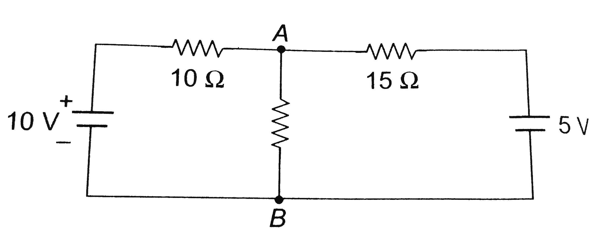 A+500mAB+1.5mAC−250mAD−500mA
In the circuit as shown in figure the
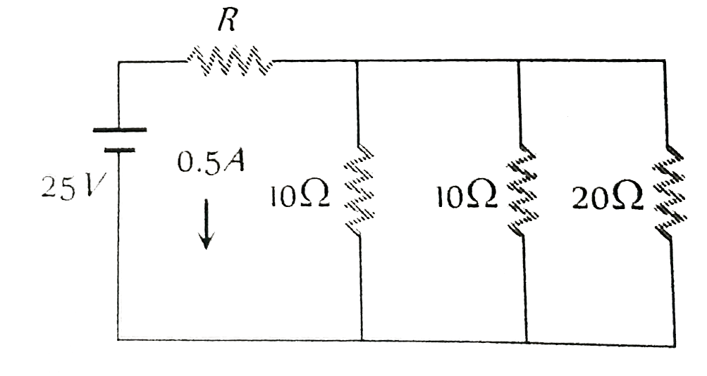 AResistance R=46ΩBCurrent through 20Ω resistance is 0.1ACPotential difference across the middle resistance is 2VDAll option are correct
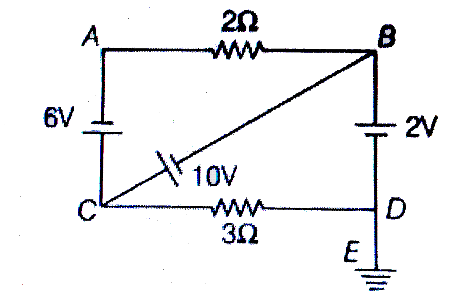
A circuit is arranged as shown in figure. The output voltage V0 is equal to ____________V.
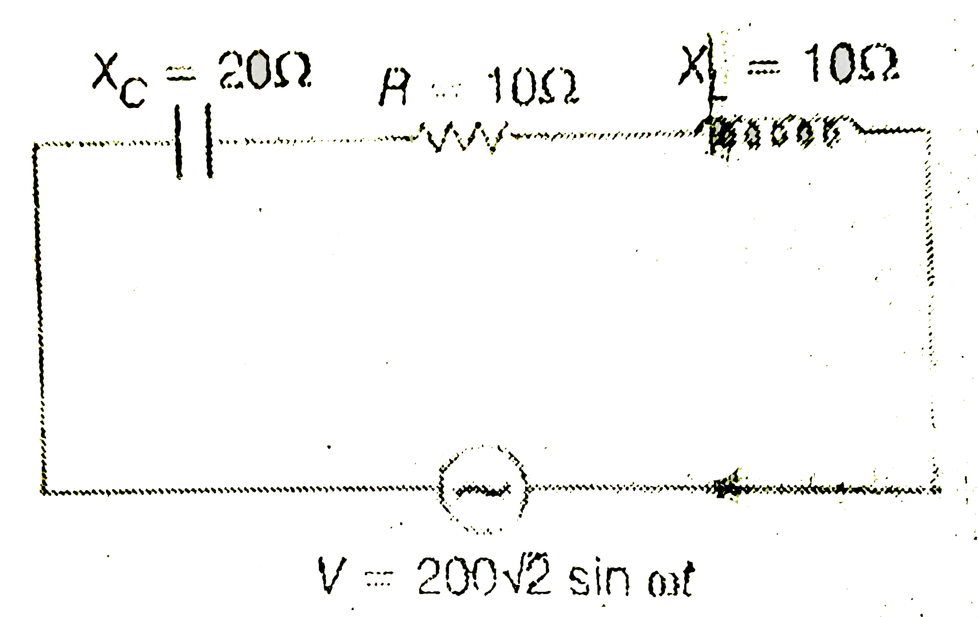
View SolutionIn LCR circuit as shown in figure
View SolutionThe circuit as shown in figure is equivalent to

View SolutionThe circuit as shown in figure is equivalent to

View SolutionIn the circuit shown in figure
View Solution

