In a p-n junction ,
A
new holes and conduction electorns are produced continuously throughout the material
B
new holes and conduction electrons are produced continuously throughout the material except in the depletion region
C
holes and conduction electrons recombine continously throughout the material
D
holes and conduction electrons recombine continuously throughout the material except in the depletion region.
Text Solution
The correct Answer is:A, D
|
Topper's Solved these Questions
- SEMICONDUCTOR AND SEMICONDUCTOR DEVICESBOOK - HC VERMACHAPTER - SEMICONDUCTOR AND SEMICONDUCTOR DEVICESEXERCISE - exercises
35 Videos
- SEMICONDUCTOR AND SEMICONDUCTOR DEVICESBOOK - HC VERMACHAPTER - SEMICONDUCTOR AND SEMICONDUCTOR DEVICESEXERCISE - Objective 2
9 Videos
- PHOTOMETRYBOOK - HC VERMACHAPTER - PHOTOMETRYEXERCISE - Exercises
16 Videos
- SPEED OF LIGHTBOOK - HC VERMACHAPTER - SPEED OF LIGHTEXERCISE - Exercises
3 Videos
Similar Questions
Knowledge Check
To make a p-n junction conducting
Athe value of forward bias should be more than the barrier potential.Bthe value of forward bias should be less than the barrier potential.Cthe value of reverse bias should be more than the barrier potential.Dthe value of reverse bias should be less than the barrier potential.The n-side of the depletion layer of a p-n junction :
Aalways has same width as of the p-side.Bhas no bound charges.Cis negatively charged.Dis positively charged.The order of thickness of depletion region in p-n junction is
A10−12mB10−6mC1mmD1 cm
In p-n junction, p-side is known as........and n-side is known as..........
View SolutionIn the forward bias arrangement of a p-n junction diode
View SolutionThe reverse saturation of p-n diode
View SolutionIn an unbiased p-n junction,
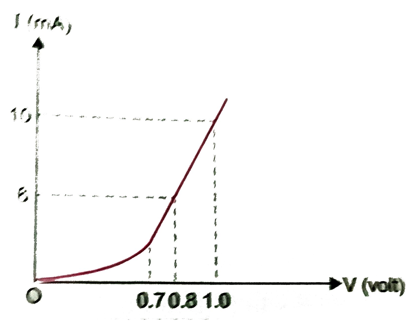
View SolutionThe forward characteristic of p-n junction is shown in Fig.What is the dynamical resistance of p-n junction at 0.9V?

View Solution
