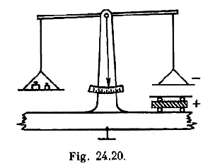
…………………….. is the appearance of an electrical potential across the sides of the crystal, when it is subjected to mechanical stress.
Text Solution
Piezoelectricity
|
Updated on:21/07/2023
Topper's Solved these Questions
- BOOK - FULL MARKSCHAPTER - SOLID STATEEXERCISE - Additional Questions (III. Match the following)5videos
SOLID STATE
- BOOK - FULL MARKSCHAPTER - SOLID STATEEXERCISE - Additional Questions (IV.Assertion and Reason)10videos
SOLID STATE
- BOOK - FULL MARKSCHAPTER - SOLID STATEEXERCISE - Additional Questions (I. Choose the best answer.)40videos
SOLID STATE
- BOOK - FULL MARKSCHAPTER - SAMPLE PAPER-8EXERCISE - PART - IV10videos
SAMPLE PAPER-8
- BOOK - FULL MARKSCHAPTER - SURFACE CHEMISTRYEXERCISE - ADDITIONAL QUESTIONS (5 Marks questions)12videos
SURFACE CHEMISTRY
Similar Questions
Knowledge Check
- Question 1 - Select One
The electrical potential difference across the resting plasma membrane is called as the
AResting potentialBAction potentialCNerve impulseDBoth B and C - Question 2 - Select One
Electricity produced on applying stress on the crystals of dielectrics is
ApiezoelectrocityBpyroelectricityCferroelectricityDantiferroelectricity - Question 3 - Select One
The electrical potential difference across the plasma memebrane at the site of depolarisation is called
AGraded potentialBResting potentialCAction potentialDNone of these
When an electric field is applied across a semiconductor,
View SolutionWhen an electric field is applied across a semiconductor,
View SolutionA spherical shell of radius R carries a uniformly distributed charge q. The electrical forces arising cause the ex-pansion of the shell. Find the mechanical stress in the shell.
 View Solution
A spherical shell of radius R carries a uniformly distributed charge q. The electrical forces arising cause the ex-pansion of the shell. Find the mechanical stress in the shell.
 View Solution
When an electric field is applied across a semiconductor,
View Solution
