(a) Draw the circuit diagram for studying the characteristics of a transistor in common
emitter configuration. Explain briefly and show how input and output characteristics
are drawn.
(b) The figure shows input weve forms A and B to a logic gate . Draw the output waveform
for an OR gate . Write the truth table for this logic gate and draw the output waveform
for an OR gate . Write truth table for this logic gate and draw its logic symbol.
(a) See Q . 30 (a) , Set-I Outside Delhi -2010.
(b) 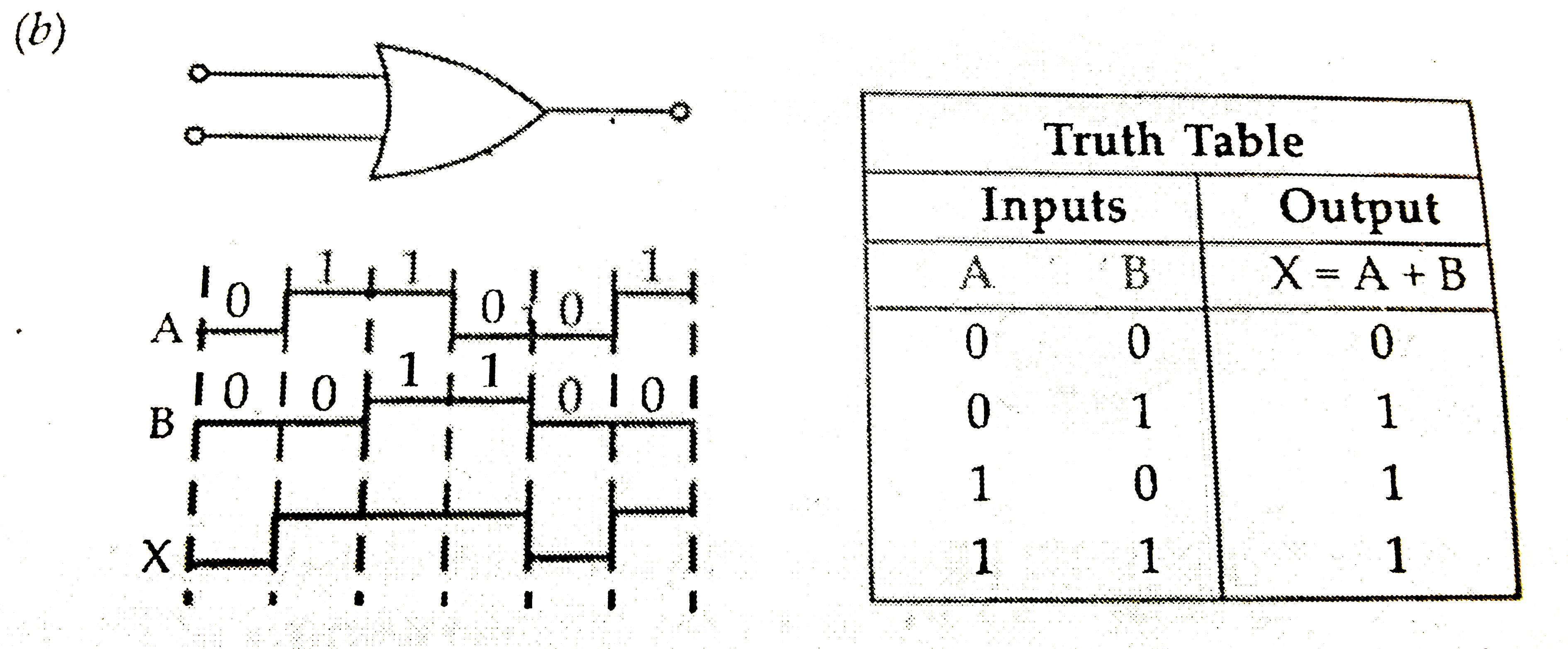 .
.
Topper's Solved these Questions
- XII BOARDSBOOK - XII BOARD PREVIOUS YEAR PAPER ENGLISHCHAPTER - XII BOARDSEXERCISE - [SET -III, OUTSIDE DELHI]
3 Videos
- XII BOARDSBOOK - XII BOARD PREVIOUS YEAR PAPER ENGLISHCHAPTER - XII BOARDSEXERCISE - SECTION - C
15 Videos
- XII BOARDSBOOK - XII BOARD PREVIOUS YEAR PAPER ENGLISHCHAPTER - XII BOARDSEXERCISE - SET-III DELHI BOARD SEC-C
5 Videos
- SAMPLE PAPER 2019BOOK - XII BOARD PREVIOUS YEAR PAPER ENGLISHCHAPTER - SAMPLE PAPER 2019EXERCISE - SECTION D
6 Videos
Similar Questions
The Fig shown input waveforms A and B to a logic gate. Draw the output waveform for an OR gate. Write the truth table for this logic gate and draw its logic symbol.
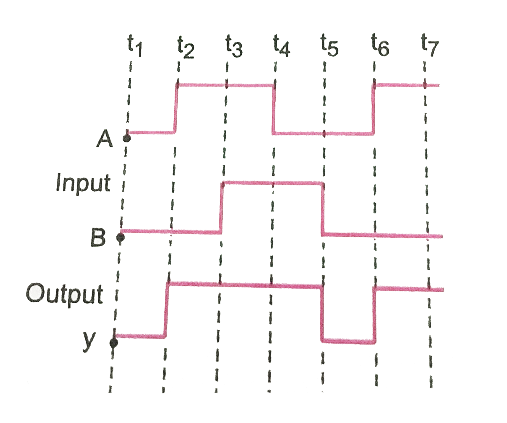
View SolutionThe Fig shown input waveforms A and B to a logic gate. Draw the output waveform for an OR gate. Write the truth table for this logic gate and draw its logic symbol.

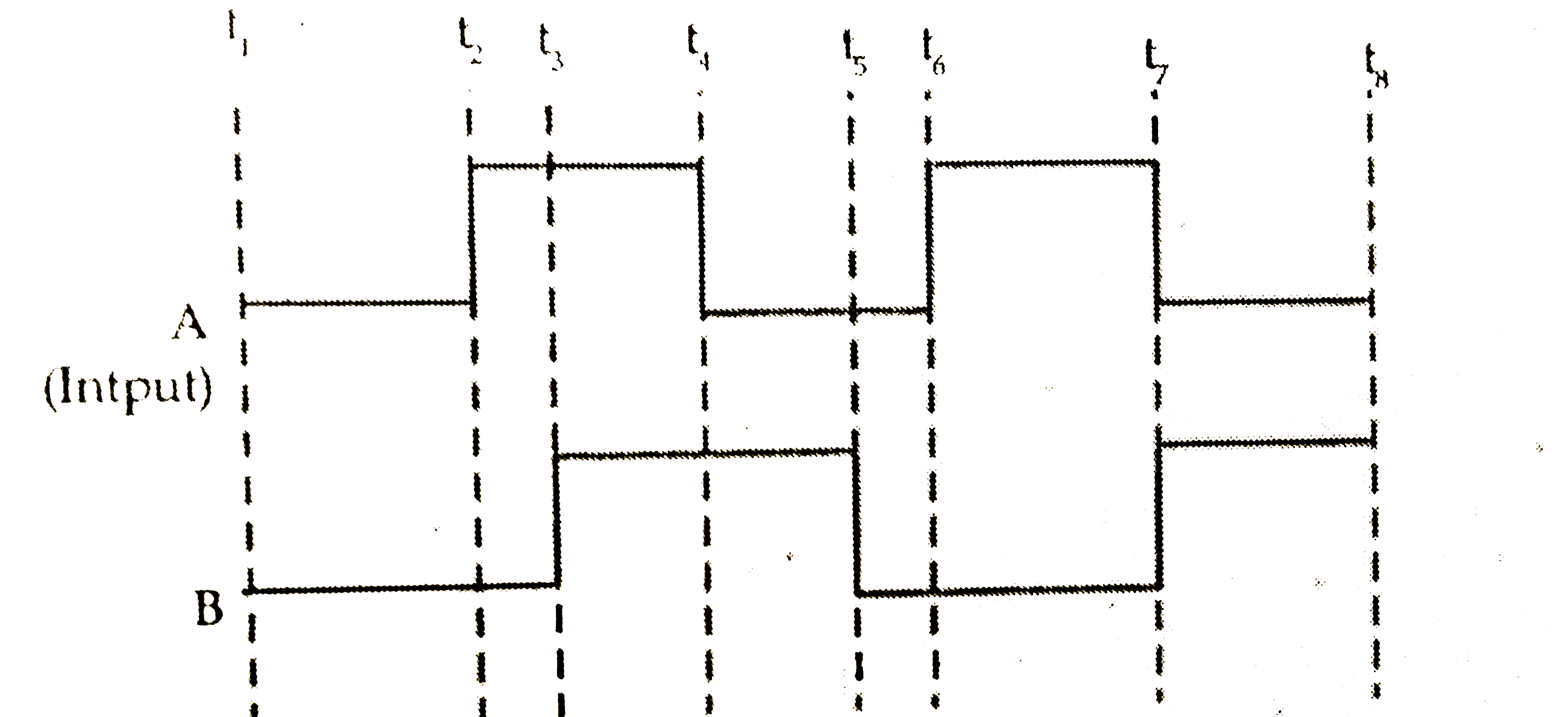
View SolutionThe figure shows the input weveforms A and B for 'AND' gate Draw the output waveform and write the truth table for this logic gate
 .
.
View SolutionThe Fig.shows the input wavwforms A and B for 'AND' gate. Draw the output waveform and write the truth table for this logic gate.
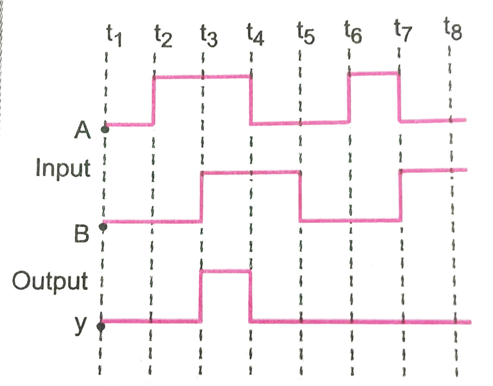
View SolutionWrite the output waveform for the gates
View SolutionWrite the output waveform of the OR gate for the inputs
View SolutionDraw a circuit diagram to study characteristics of a transistor (pnp or ppn) in common emitter configuration. Draw the sketch of (i) input characterisitics and (ii) output characteristics for this configuration.
View Solution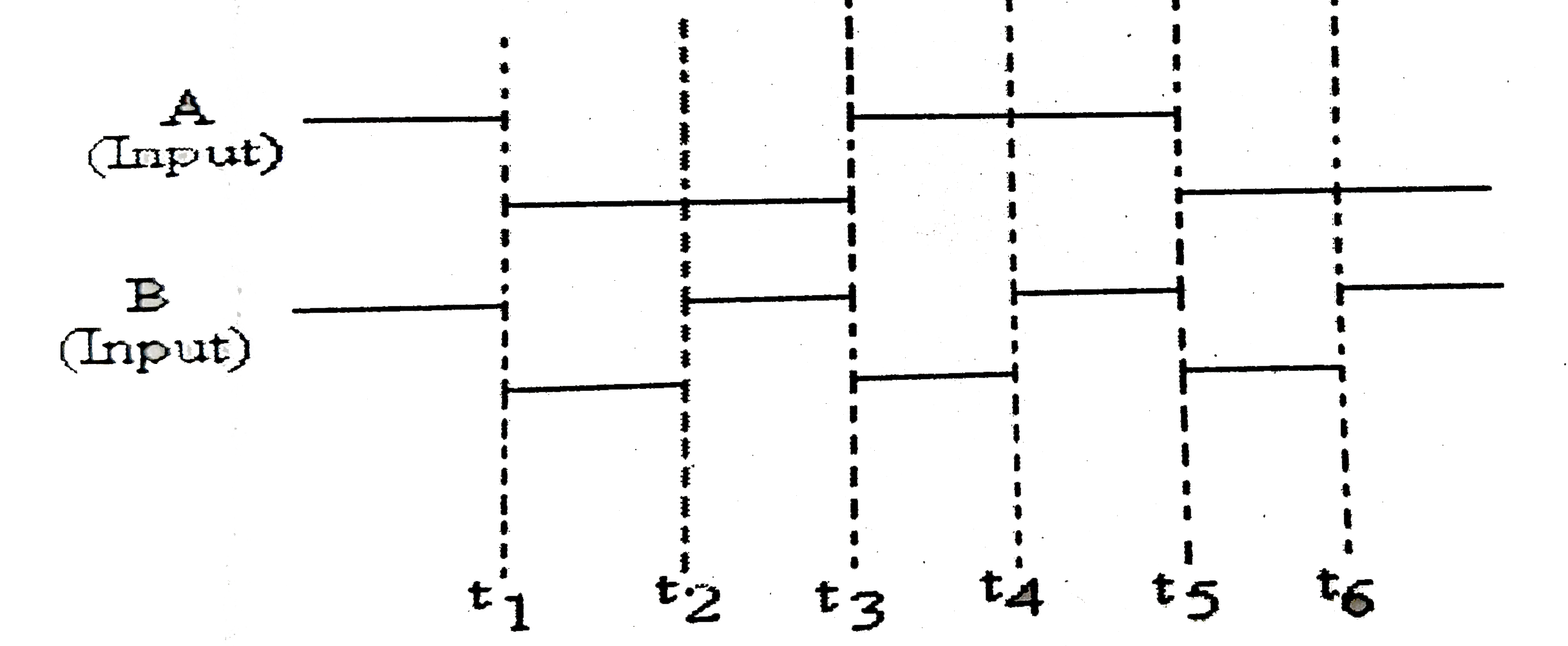
The give inputs A, B are fed to a 2-input NAND gate. Draw the output wave form of the gate.
View Solution
The give inputs A, B are fed to a 2-input NAND gate. Draw the output wave form of the gate.
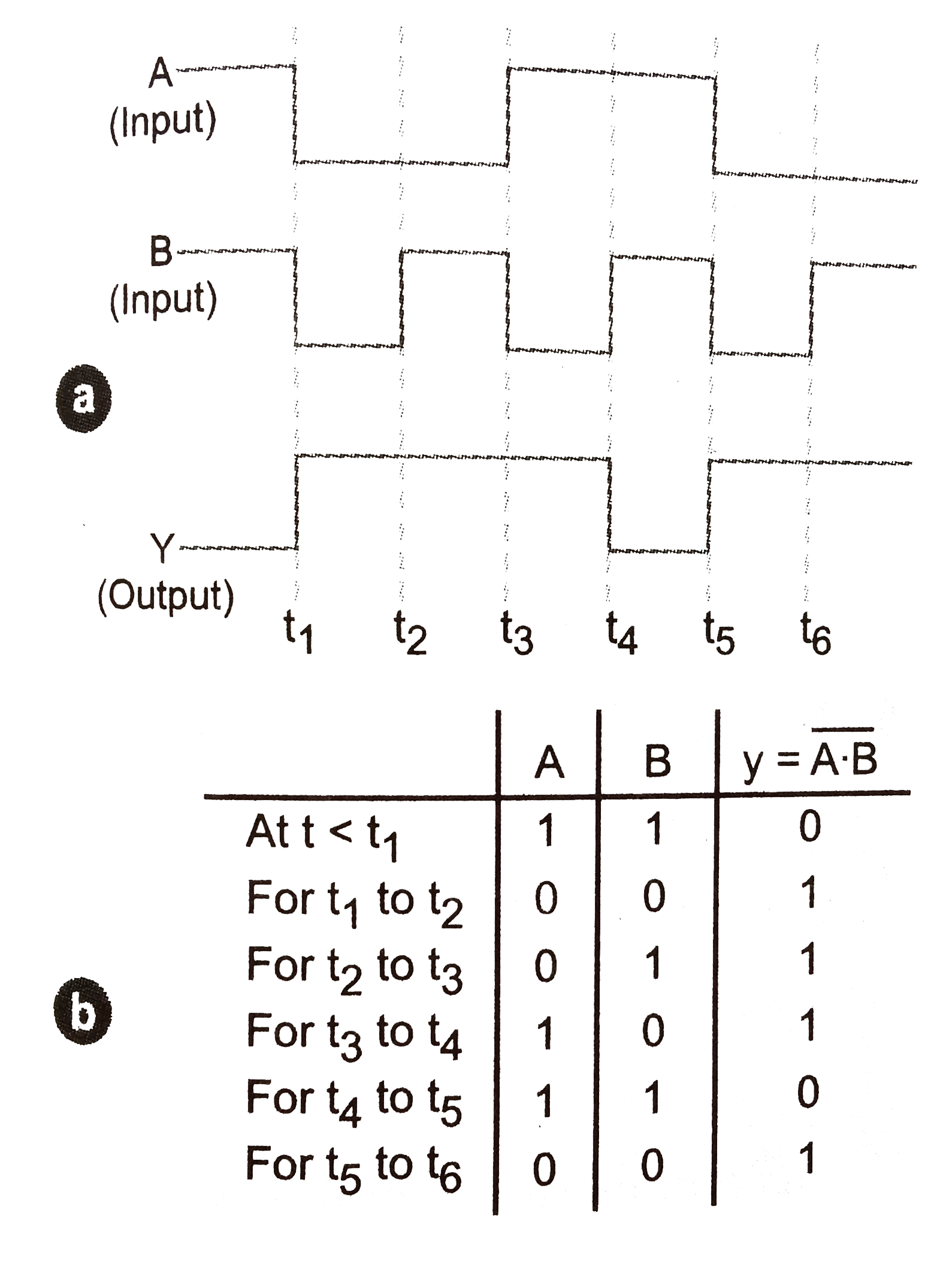
View SolutionThe following Fig. shows the input waveforms (A,B) and the output waveform (y) of a gate. Identify the gate and write its truth table.
View Solution
