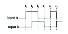
As shown in the following figure take A and B input waveforms. Sketch the output waveform obtained from NAND gate.
 Solution in Gujrati
NAND gate
OR gate
NOR gate
AND gate
The correct Answer is:B
Step by step video & image solution for As shown in the following figure take A and B input waveforms. Sketch the output waveform obtained from NAND gate. by Physics experts to help you in doubts & scoring excellent marks in Class 12 exams.
Updated on:21/07/2023Topper's Solved these Questions
- SEMICONDUCTOR ELECTRONICS : MATERIALS, DEVICES AND SIMPLE CIRCUITS BOOK - KUMAR PRAKASHANCHAPTER - SEMICONDUCTOR ELECTRONICS : MATERIALS, DEVICES AND SIMPLE CIRCUITS EXERCISE - Section-D : Multiple Choice Questions (MCQs) (MCQs From .DARPAN. Based On Textbook)
116 Videos
- SAMPLE QUESTION PAPER BOOK - KUMAR PRAKASHANCHAPTER - SAMPLE QUESTION PAPER EXERCISE - PART-B SECTION-C
5 Videos
- WAVE OPTICSBOOK - KUMAR PRAKASHANCHAPTER - WAVE OPTICSEXERCISE - SECTION-D (MULTIPLCE CHOICE QUESTIONS (MCQS)) (MCQS FROM DARPAN BASED ON TEXTBOOK)
239 Videos
Similar Questions
Which of the following is not a conductor of electricity?
View SolutionTwo charges –q and +q are located at points (0, 0, –a) and (0, 0, a), respectively.
(a) What is the electrostatic potential at the points (0, 0, z) and (x, y, 0) ?
(b) Obtain the dependence of potential on the distance r of a point from the origin when r/a>>1 .
(c) How much work is done in moving a small test charge from the point (5,0,0) to (–7,0,0) along the x-axis? Does the answer change if the path of the test charge between the same points is not along the x-axis?
View SolutionAccording to particle theory of light what is the velocity of light in a dense medium, compared to that in rare medium ?
View Solutionनीचे दिखाये गए निवेश A तथाB के लिएNAND गेट के निर्गत तरंग -रूप को स्केच कीजिये ।
View SolutionSketch the output waveform Y from a NAND gate having following inputs A and B
View SolutionSketch the output waveform obtained from AND gate for the following inputs A and B.
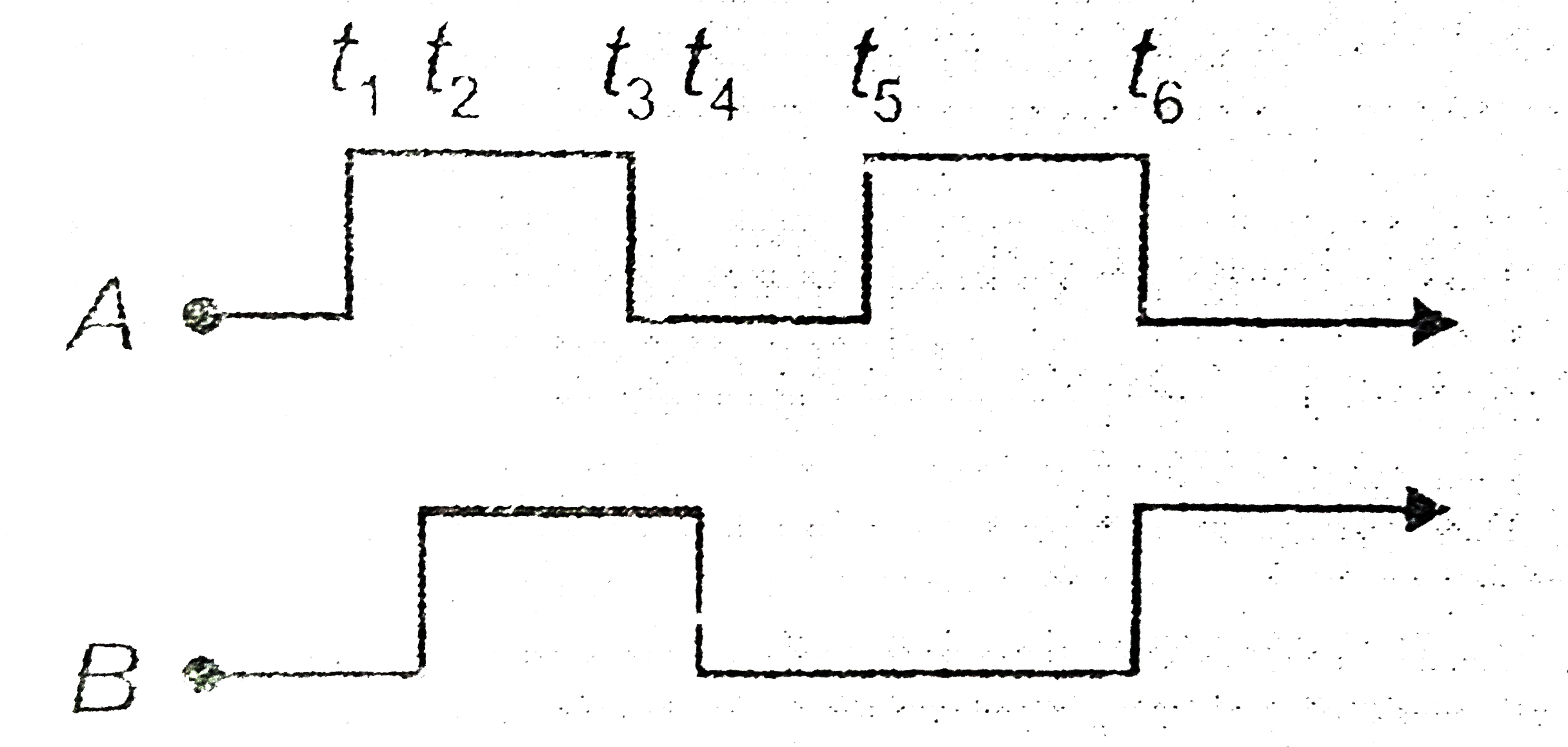
View Solutionसंलग्न चित्र में A तथा B , दो निवेशी OR गेट तथा NAND गेट के निवेशी तरंग प्रतिरूप हैं। दोनों गेटों के निर्गत तरंग प्रतिरूप ( Y ) अपनी उत्तर पुस्तिका में दर्शाइये।
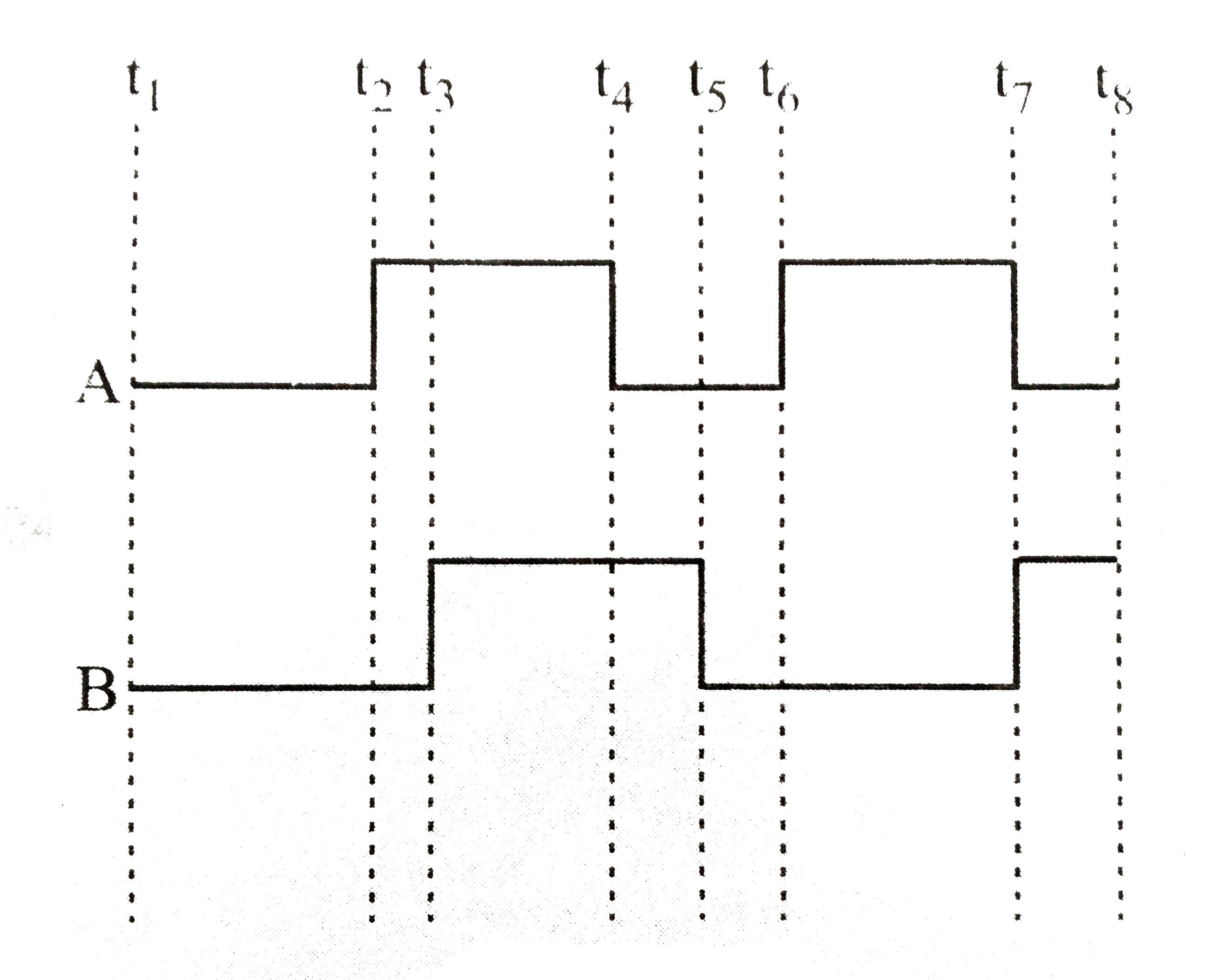
View SolutionTake A and B input waveforms similar to that in Example .Sketch the output waveform obtained from AND gate.
View SolutionTake X and Y input waveforms. Sketch the output (Z) waveform abtained from AND gate as per the following conditions:
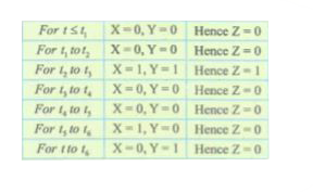
View SolutionSketch the output waveform obtained from AND gate for the following inputs A and B.

View SolutionTake A and B input waveforms similar to that in Ex. Sketch the output waveform obtained from AND gate .
View SolutionTake A and B input waveforms similar to that in Example. Sketch the output waveform obtained from AND gate.
View SolutionTake A and B input waveforms similar to that in Example. Sketch the output waveform obtained from AND gate.
View SolutionTake A and B input waveforms similar to that in Example. Sketch the output waveform obtained from AND gate.
View SolutionTake A and B input waveforms similar to that in Example. Sketch the output waveform obtained from AND gate.
View SolutionThe digital signal for the OR gate with two inputs is shown in the figure. Sketch the output waveform obtained from OR gate.
View Solution
