Can the potential barrier across a p−n junction be measured by simply connecting a voltmeter across the junction ?
Because there is no free charge carrier in depletion region.
Topper's Solved these Questions
- ELECTRONIC DEVICES BOOK - CBSE COMPLEMENTARY MATERIALCHAPTER - ELECTRONIC DEVICES EXERCISE - SHORT ANSWER QUESTIONS (3 MARKS)
7 Videos
- ELECTRONIC DEVICES BOOK - CBSE COMPLEMENTARY MATERIALCHAPTER - ELECTRONIC DEVICES EXERCISE - LONG ANSWER QUESTIONS (5 MARKS)
1 Videos
- ELECTRONIC DEVICES BOOK - CBSE COMPLEMENTARY MATERIALCHAPTER - ELECTRONIC DEVICES EXERCISE - NUMERICALS
7 Videos
- ELECTROMAGNETIC WAVES AND OPTICSBOOK - CBSE COMPLEMENTARY MATERIALCHAPTER - ELECTROMAGNETIC WAVES AND OPTICSEXERCISE - 1 mark question
11 Videos
- ELECTROSTATICS AND CURRENT ELECTRICITY BOOK - CBSE COMPLEMENTARY MATERIALCHAPTER - ELECTROSTATICS AND CURRENT ELECTRICITY EXERCISE - NUMERICALS
49 Videos
Similar Questions
Knowledge Check
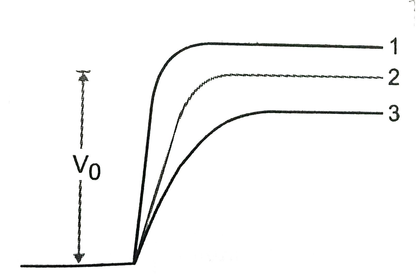
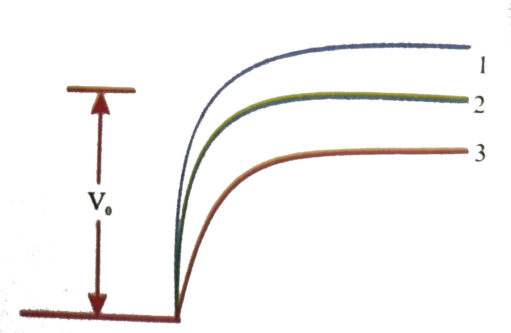
In Fig . V0 is the potential barrier across a p-n junction, when no battery is connected across the junction
 A1 and 3 both correspond to forward bias of junctionB3 corresponds to forward bias of junction and 1 corresponds to reverse bias of junctionC1 corresponds to forward bias and 3 corresponds to reverse bias of junctionD3 and 1 both correspond to reverse bias of junction
In Fig. V0 is the potential barrier across a p−n junction, when no battery is connected across the junction :
 .A1 and 3 both correspond is forward bias of junctionB3 corresponds to forward bias of junction and 1 corresponds to reverse bias junctionC1 corresponds to forward bias and 3 corresponds to reverse bias junctionD3 and 1 both correspond to reverse bias and 3 corresponds to revers bias of junction
The potential barrier at PN junction is due to
Afixed acceptor and donor ions on either side of the junctionBminority carriers on either side of the junctionCmajority carriers on either side of the junctionDboth majority and minority carriers on either side of junction
p-n junction is a semiconductor diode. It is obtained by bringing p-type semiconductor inclose contact with n-type semiconductor. A thin layer is developed at the p-n junction which is devoid of any charge carrier but has immobile ions. It is called depletion layer. At the junction a potential barrier appears, which does not allow the movement of majority charge carriers across the junction in the absence of any biasing of the junction.
p-n junction offer low resistance when forward biased and high resistance when reverse biased. Read the above paragaph and answer the following question:
(i) Can we measure the potential barrier of p-n junction by putting a sensitive voltmeter across its terminals?
(ii) What practical lesson do you draw from the above study?
View SolutionCan we measure the potential difference of a p-n junction by putting a sensitive voltmeter across its terminals?
View SolutionPotential barrier developed in a junction diode opposes
View SolutionAssertion: We can measure the potential barrier of a PN junction by putting a sensitive voltmeter across its terminals.
Reason: The current through the PN junction is not same in forward and reversed bias.
View SolutionAssertion : We cannot meausre that potential barrier of p-n junction by putting a sensitive voltmeter across its terminals.
Reason: In the depletion layer, there are no free elctrons or holes and in the absence of forward bias, it offers, infinite, resistance.
View Solution
