Consider the following statements A and B and identify the correct answer : A: A Zener diode is always connected in reverse bias. B: The potential barrier of a P-n junction lies in between 0.1 to 0.7 volts, approximately.
A is true, B is false
A is false, B is true
A and B are true
A and B are false
The correct Answer is:C
To solve the question, we need to analyze the two statements A and B regarding Zener diodes and the potential barrier of a P-N junction.
Step 1: Analyze Statement A
Statement A states that "A Zener diode is always connected in reverse bias."
- Explanation: A Zener diode is specifically designed to operate in reverse bias. When reverse-biased, it allows current to flow when the voltage exceeds a certain value known as the Zener breakdown voltage. This characteristic makes it useful for voltage regulation in circuits.
Conclusion for Statement A: This statement is correct.
Step 2: Analyze Statement B
Statement B states that "The potential barrier of a P-N junction lies in between 0.1 to 0.7 volts, approximately."
- Explanation: The potential barrier (or built-in potential) of a P-N junction depends on the materials used. For silicon, the potential barrier is typically around 0.6 to 0.7 volts, and for germanium, it is about 0.3 to 0.4 volts. The range mentioned in Statement B (0.1 to 0.7 volts) is misleading because it suggests a lower limit that does not accurately represent the typical values for common semiconductor materials.
Conclusion for Statement B: This statement is incorrect.
Step 3: Identify the Correct Answer
Based on the analysis:
- Statement A is correct.
- Statement B is incorrect.
Thus, the correct answer is that only Statement A is correct.
Final Answer
The correct answer is Statement A is correct, Statement B is incorrect.
---
Statement A states that "A Zener diode is always connected in reverse bias."
Statement B states that "The potential barrier of a P-N junction lies in between 0.1 to 0.7 volts, approximately."
Based on the analysis:
- Statement A is correct.
- Statement B is incorrect.
The correct answer is Statement A is correct, Statement B is incorrect.
Topper's Solved these Questions
- SEMICONDUCTOR DEVICESBOOK - AAKASH SERIESCHAPTER - SEMICONDUCTOR DEVICESEXERCISE - EXERCISE -I (ASSERTION & REASON)
12 Videos
- SEMICONDUCTOR DEVICESBOOK - AAKASH SERIESCHAPTER - SEMICONDUCTOR DEVICESEXERCISE - EXERCISE -II (ENERGY BANDS AND CLASSIFICATION OF SOLIDS )
3 Videos
- SEMICONDUCTOR DEVICESBOOK - AAKASH SERIESCHAPTER - SEMICONDUCTOR DEVICESEXERCISE - EXERCISE -I (MATCHING TYPE QUESTIONS)
9 Videos
- RAY OPTICSBOOK - AAKASH SERIESCHAPTER - RAY OPTICSEXERCISE - PROBLEMS ( LEVEL-II)
60 Videos
- UNITS AND MEASUREMENTBOOK - AAKASH SERIESCHAPTER - UNITS AND MEASUREMENTEXERCISE - PRACTICE EXERCISE
45 Videos
Similar Questions
Consider the following statements A and B and identify the correct answer
(A) A Zener diode is always connected in reverse bias to use it as voltage regulator.
(B) The potential barrier of a p−n junction lies between 0.1 to 0.3V, approximately.
View SolutionConsider the following statement A and B and identify the correct answer
A) Radio waves diffract around buildings but light waves does not
B) To cut down glare of incident light we prefer sun glasses made from polaroids
View Solution
Knowledge Check
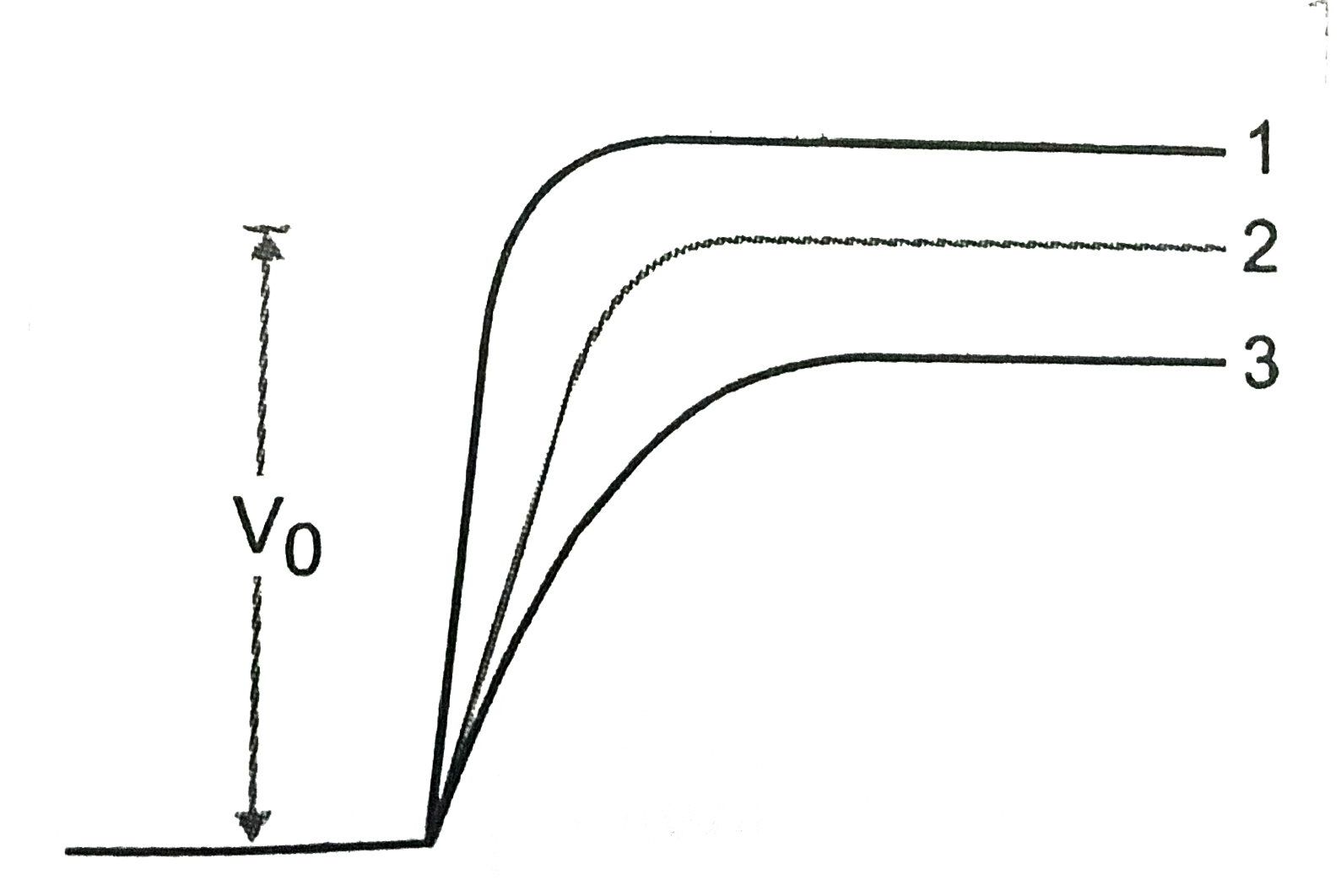
In Fig . V0 is the potential barrier across a p-n junction, when no battery is connected across the junction
 A1 and 3 both correspond to forward bias of junctionB3 corresponds to forward bias of junction and 1 corresponds to reverse bias of junctionC1 corresponds to forward bias and 3 corresponds to reverse bias of junction.D3 and 1 both correspond to reverse bias of junction.
Consider the following statement A and B and identify the correct answer
A) In the case of narrow source of light coherent sources are obtained by the division of wave front
B) Diffraction is due to interference of light from secondary sources of the same wave front whereas interference is due to superposition of two waves derived from the same source.
View SolutionConsider the following two statements A and B and identify the correct answer given below.
A. Nuclear density is same for all nuclei.
B.Radius of the nucleus R and its mass number A are related as √AαR16.
View SolutionConsider the following two statements A and B and identify the correct choice in the given answer
A : The characteristic X-ray spectrum depends on the nature of the material of the target
B : The short wavelength limit of continuous X-ray spectrum varies inversely with the potential difference applied to the X-rays tube
View SolutionConsider the following statements (A) and (B) and identify the correct answer given below.
Statement (A): Positive values of packing fraction implies a large value of binding energy.
Statement (B): The difference between the mass of the nucleus and the mass number of the nucleus is called packing fraction
View SolutionIn Fig . V0 is the potential barrier across a p-n junction, when no battery is connected across the junction

View SolutionConsider the following statements. A, B and identify the correct choice in the given answers
(A) Density of a nucleus is independent of its mass number
(B) Beryllium is used as moderator in nuclear reactors
View SolutionBy giving counter example show that following statement are false
(a) p : Square of a real number is always integer
(b) p : The equation x2−9=0 does not have a root lying between 0 and 4
View Solution
