Consider the following statements A and B and identify the correct answer
(A) A Zener diode is always connected in reverse bias to use it as voltage regulator.
(B) The potential barrier of a p−n junction lies between 0.1 to 0.3V, approximately.
a. [1] and [2] are correct
b. [1] and [2] are wrong
c. [1] is correct, but [2] is wrong
d. [1] is wrong, but [2] is correct
The correct Answer is:C
To solve the question, we need to analyze the two statements (A and B) regarding Zener diodes and the potential barrier of p-n junctions.
Step 1: Analyze Statement A
- Statement A: "A Zener diode is always connected in reverse bias to use it as a voltage regulator."
- Explanation: A Zener diode is specifically designed to operate in reverse bias. When connected in reverse bias, it maintains a constant voltage across it (known as the Zener voltage) despite changes in the load current. This property makes it ideal for use as a voltage regulator.
- Conclusion: Statement A is True.
Step 2: Analyze Statement B
- Statement B: "The potential barrier of a p-n junction lies between 0.1 to 0.3 V, approximately."
- Explanation: The potential barrier (also known as the built-in potential) of a p-n junction varies depending on the semiconductor material. For silicon-based diodes, the potential barrier is typically around 0.6 to 0.7 V, while for germanium-based diodes, it is approximately 0.3 to 0.35 V. Thus, the statement suggesting a range of 0.1 to 0.3 V is incorrect.
- Conclusion: Statement B is False.
Step 3: Determine the Correct Answer
- Based on the analysis:
- Statement A is True.
- Statement B is False.
- Therefore, the correct answer is that Statement A is correct and Statement B is incorrect.
Final Answer
The correct option is C: 1 correct and 2 is wrong.
---
- Statement A: "A Zener diode is always connected in reverse bias to use it as a voltage regulator."
- Explanation: A Zener diode is specifically designed to operate in reverse bias. When connected in reverse bias, it maintains a constant voltage across it (known as the Zener voltage) despite changes in the load current. This property makes it ideal for use as a voltage regulator.
- Conclusion: Statement A is True.
- Statement B: "The potential barrier of a p-n junction lies between 0.1 to 0.3 V, approximately."
- Explanation: The potential barrier (also known as the built-in potential) of a p-n junction varies depending on the semiconductor material. For silicon-based diodes, the potential barrier is typically around 0.6 to 0.7 V, while for germanium-based diodes, it is approximately 0.3 to 0.35 V. Thus, the statement suggesting a range of 0.1 to 0.3 V is incorrect.
- Conclusion: Statement B is False.
- Based on the analysis:
- Statement A is True.
- Statement B is False.
- Therefore, the correct answer is that Statement A is correct and Statement B is incorrect.
The correct option is C: 1 correct and 2 is wrong.
Topper's Solved these Questions
- SEMICONDUCTORSBook:RESONANCE ENGLISHChapter:SEMICONDUCTORSExercise:Exercise 2
Explore 16 Videos
- SEMICONDUCTORSBook:RESONANCE ENGLISHChapter:SEMICONDUCTORSExercise:Exercise 3
Explore 88 Videos
- SEMICONDUCTORSBook:RESONANCE ENGLISHChapter:SEMICONDUCTORSExercise:Exercise 3
Explore 88 Videos
- REVISION DPPBook:RESONANCE ENGLISHChapter:REVISION DPPExercise:All Questions
Explore 463 Videos
- SIMPLE HARMONIC MOTION Book:RESONANCE ENGLISHChapter:SIMPLE HARMONIC MOTION Exercise:Advanced Level Problems
Explore 13 Videos
Similar Questions
Consider the following statements. A, B and identify the correct choice in the given answers
(A) Density of a nucleus is independent of its mass number
(B) Beryllium is used as moderator in nuclear reactors
View SolutionConsider the following two statements A and B and identify the correct answer given below.
A. Nuclear density is same for all nuclei.
B.Radius of the nucleus R and its mass number A are related as √AαR16.
View Solution
Knowledge Check
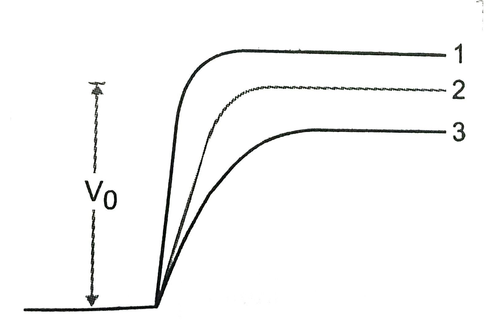
In Fig . V0 is the potential barrier across a p-n junction, when no battery is connected across the junction
 A1 and 3 both correspond to forward bias of junctionB3 corresponds to forward bias of junction and 1 corresponds to reverse bias of junctionC1 corresponds to forward bias and 3 corresponds to reverse bias of junction.D3 and 1 both correspond to reverse bias of junction.
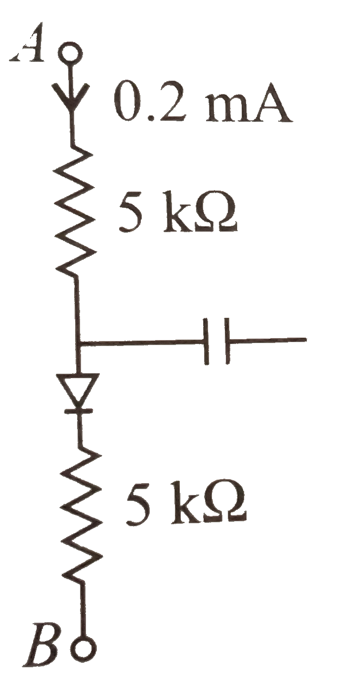
In the circuit shown in figure, if the A diode forward voltage drop is 0.3 V, the voltage difference between A and B is
 A1.3 VB2.3 VC0D0.5 V
Consider the following statement A and B and identify the correct answer
A) Fresnel.s diffraction pattern occurs when the source of light or the screen on which the diffraction pattern is seen or when both are at finite distance from the aperture
B) Diffraction light can be used to estimate the helical structure of nucleic acids
View SolutionConsider the following statements (A) and (B) and identify the correct answer given below.
Statement (A): Positive values of packing fraction implies a large value of binding energy.
Statement (B): The difference between the mass of the nucleus and the mass number of the nucleus is called packing fraction
View SolutionConsider the following two statements A and B and identify the correct choice in the given answer
A : The characteristic X-ray spectrum depends on the nature of the material of the target
B : The short wavelength limit of continuous X-ray spectrum varies inversely with the potential difference applied to the X-rays tube
View SolutionIn Fig . V0 is the potential barrier across a p-n junction, when no battery is connected across the junction

View SolutionIn V-I characteristics of a p-n junction diode, why is the current under reverse bias almost independent of the applied potential upto a critical voltage?
View SolutionIn the circuit shown in figure, if the diode forward voltage drop is 0.3 V, then the voltage difference between A to B is,

View Solution