Discuss how a NOT gate is realised using NAND gates.
Video Solution
Text Solution
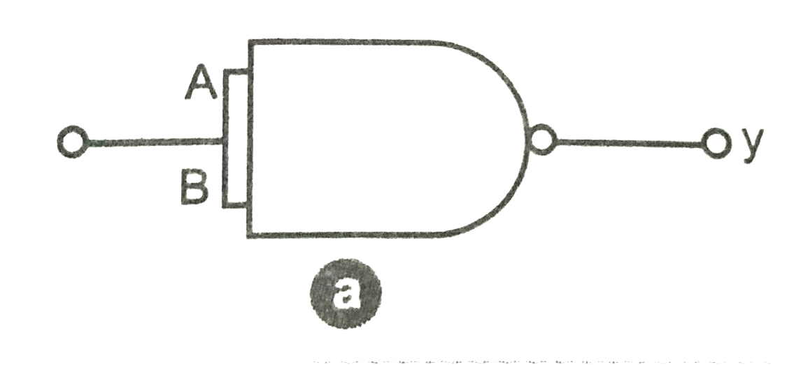
If the two input of the NAND gates are joined to make one input as shown in Fig, then the NAND gate function as a NOT gate. As
y=¯¯¯¯¯¯¯¯A.A=¯¯¯A+¯¯¯A=¯¯¯A
In the truth table of NAND gate, if we use B=A, we obtain the truth table as given in Fig., which is the truth table of NOT gate.

∣∣
∣∣AB=AY001110∣∣
∣∣
|
Topper's Solved these Questions
- ELECTRONIC DEVICESBOOK - PRADEEPCHAPTER - ELECTRONIC DEVICESEXERCISE - SAMPLE PROBLEM
2 Videos
- ELECTRONIC DEVICESBOOK - PRADEEPCHAPTER - ELECTRONIC DEVICESEXERCISE - CONCEPTUAL PROBLEMS
1 Videos
- ELECTROMAGNETIC WAVESBOOK - PRADEEPCHAPTER - ELECTROMAGNETIC WAVESEXERCISE - II Focus multiple choice question
5 Videos
- ELECTROSTATICSBOOK - PRADEEPCHAPTER - ELECTROSTATICSEXERCISE - ASSERTION-REASON TYPE QUESTIONS
2 Videos
Similar Questions
Knowledge Check
NAND gate is-
Aa basic gateBnot a universal gateCa universal gateDa universal gateHow many NOR gates are used to form an AND gate
A1B2C3D4Statement 1: If output of a AND gate is fed to OR gate, it is called NOR gate.
Statement 2: If output of a AND gate is fed to NOT gate, it is called NAND gate.AStatement 1 is True, Statement -2 is true,
Statement -2 is a correct explanation for statement 1:BStatement-1 is True, Statement -2 is True,
Statement 2 is Not a correct explanation for statement -1CStatement 1 is True, Statement -2 is FalseDStatement 1 is False Statement 2 is True
How a NOR gate is formed
View SolutionDicuss how the OR gate is realised from the NOR gate.
View SolutionDicuss how the AND gate is realised from the NOR gate.
View SolutionHow is NOT gate realised? Explain.
View SolutionWrite the truth table of a two input NOR gate. Explain, using a logic circuit, how a NOR gate can be converted into an AND gate.
View Solution
