Explain the forward characteristics of the p-n junction diode by drawing circuit and graph. Solution in Gujrati
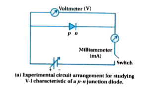
The configuration of the circuit for the p-n junction diode forward characteristics is shown in the figure.

The battery is connected to the diode through a potentiometer (or reheostat) so that the applied voltage to the directed can be changed.
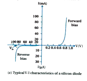
For different values of voltages, the value of the current in noted. A graph between V→I is obtained in first quadrant for Si diode as shown in figure. Here, current is of the order of mA.

In forward bias, the current first increases very slowly, (almost neglibible) till the voltage across the diode crosses a certain value.
After the characteristic voltage, the diode current increases exponentially, even for a very small increase in the diode bias voltage. This voltage is called the thershold voltage or cut-in voltage.
~0.2 V for germanium diode and −07 V for silicon diode.
Usually the p-n junction diode current flow in one direction so it is used for rectification of A.C. voltage.
If the forward voltage is increased beyond the value of its safety voltage a very large current is generated so overheating can cause the p-n junction diode to be destroyed. Junction diodes of Ge or Si do not cause any damage to the 100∘Cand170∘C temperatures respectively.
Topper's Solved these Questions
- SEMICONDUCTOR ELECTRONICS : MATERIALS, DEVICES AND SIMPLE CIRCUITS BOOK - KUMAR PRAKASHANCHAPTER - SEMICONDUCTOR ELECTRONICS : MATERIALS, DEVICES AND SIMPLE CIRCUITS EXERCISE - Section-B : Numericals (Numerical From Textual illustrations)
16 Videos
- SEMICONDUCTOR ELECTRONICS : MATERIALS, DEVICES AND SIMPLE CIRCUITS BOOK - KUMAR PRAKASHANCHAPTER - SEMICONDUCTOR ELECTRONICS : MATERIALS, DEVICES AND SIMPLE CIRCUITS EXERCISE - Section-B : Numericals (Numerical From Textual Exercise)
15 Videos
- SEMICONDUCTOR ELECTRONICS : MATERIALS, DEVICES AND SIMPLE CIRCUITS BOOK - KUMAR PRAKASHANCHAPTER - SEMICONDUCTOR ELECTRONICS : MATERIALS, DEVICES AND SIMPLE CIRCUITS EXERCISE - Section-D : Multiple Choice Questions (MCQs) (MCQs asked in Competitive Exams)
129 Videos
- SAMPLE QUESTION PAPER BOOK - KUMAR PRAKASHANCHAPTER - SAMPLE QUESTION PAPER EXERCISE - PART-B SECTION-C
5 Videos
- WAVE OPTICSBOOK - KUMAR PRAKASHANCHAPTER - WAVE OPTICSEXERCISE - SECTION-D (MULTIPLCE CHOICE QUESTIONS (MCQS)) (MCQS FROM DARPAN BASED ON TEXTBOOK)
239 Videos
Similar Questions
C, Si and Ge have same lattice structure. Why is C insulator while Si and Ge intrinsic semiconductors?
View SolutionIn an n type silicon, which of the following statements is true:
View SolutionAt absolute zero temperature Si acts as ……..
View SolutionTwo charges –q and +q are located at points (0, 0, –a) and (0, 0, a), respectively.
(a) What is the electrostatic potential at the points (0, 0, z) and (x, y, 0) ?
(b) Obtain the dependence of potential on the distance r of a point from the origin when r/a>>1 .
(c) How much work is done in moving a small test charge from the point (5,0,0) to (–7,0,0) along the x-axis? Does the answer change if the path of the test charge between the same points is not along the x-axis?
View SolutionAccording to particle theory of light what is the velocity of light in a dense medium, compared to that in rare medium ?
View SolutionExplain briefly with the help of necessary diagram, the forward and the reverse biasing of p-n junction diode. Also draw their characteristic curves in the two cases.
View Solutionp - n सन्धि डायोड का अग्र दिशिक परिपथ बनाइए ।
View SolutionExplain the working of p-n junction diode in forward and reverse biased mode.
View SolutionDraw the circuit diagram of a forward biased and reverse biased p-n junction diode.
View SolutionDraw the graph showing the variation of current with voltage for a p-n junction diode in forward bias as well as revese bias arrangements.
View SolutionDraw the circuit arrangement for studying the V - I characteristics of a p-n junction diode in (i) forward and (ii) reverse bias. Briefly explain how the typical V - I characteristics of a diode are obtained and draw these characteristics.
View SolutionExplain the reverse characteristics of p-n junction diode by circuit diagram with graph.
View SolutionExplain briefly with the help of necessary diagram, the forward and the reverse biasing of p-n junction diode. Also draw their characteristic curves in the two cases.
View SolutionWith the help of circuit diagram, explain theV-l characteristics of p-n junction diode in forward biasing.
View SolutionWith the help of circuit diagram, explaintheV-l characteristics of p-n junction diode in forward biasing.
View Solution
