Explain the use of junction diode as a full wave rectifier by drawing circuit diagram and draw the form of input and output waves. Solution in Gujrati
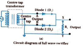
The full wave rectifier is made of a transformer, two junction diode D1andD2 and a load resistance RL.

The primary coil of the transformer is connected to the a.c. supply. The p-side of the two diodes are connected to the ends of the secondary of the transformer and both diodes are connected to the centre tap of the secondary by attaching the n-sides to the load resistance RL.
Each diode works only during half of the full cycle of a.c. simultaneously, and therefore during the full cycle of a.c. between the two ends of load resistance RL, the current obtain in one direction which is called rectified (unidirectional) current.
Full wave rectification can also be obtained using four junction diodes, which does not required a centre tap in the secondary.
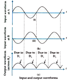
The voltage at B becomes positive during a.c. cycles when the voltage at A relative to the centre tap becomes negative so current does not flow from D1 (due to reverse bias) but current flow from D2 (due to forward bias) and current flow from load resistance RL in X to Y direction.
And when the diode A becomes forward bias and B becomes reverse bias during a.c. cycle, the current does not flow from diode B but current is flow in A so the current flows from load resistance RL in the X to Y direction.
Hence, current flows from both diode simultaneously occur during the subsequent a.c. cycle hence flows load resistance in one direction so D.C. voltage across the resistance is obtained.
The input of both diode and the output waveform obtain from RL in full wave rectifier is shown in below figure (c ).

The efficiency of a full wave rectifier is higher than the efficiency of a halfwave rectifier.
Topper's Solved these Questions
- SEMICONDUCTOR ELECTRONICS : MATERIALS, DEVICES AND SIMPLE CIRCUITS BOOK - KUMAR PRAKASHANCHAPTER - SEMICONDUCTOR ELECTRONICS : MATERIALS, DEVICES AND SIMPLE CIRCUITS EXERCISE - Section-B : Numericals (Numerical From Textual illustrations)
16 Videos
- SEMICONDUCTOR ELECTRONICS : MATERIALS, DEVICES AND SIMPLE CIRCUITS BOOK - KUMAR PRAKASHANCHAPTER - SEMICONDUCTOR ELECTRONICS : MATERIALS, DEVICES AND SIMPLE CIRCUITS EXERCISE - Section-B : Numericals (Numerical From Textual Exercise)
15 Videos
- SEMICONDUCTOR ELECTRONICS : MATERIALS, DEVICES AND SIMPLE CIRCUITS BOOK - KUMAR PRAKASHANCHAPTER - SEMICONDUCTOR ELECTRONICS : MATERIALS, DEVICES AND SIMPLE CIRCUITS EXERCISE - Section-D : Multiple Choice Questions (MCQs) (MCQs asked in Competitive Exams)
129 Videos
- SAMPLE QUESTION PAPER BOOK - KUMAR PRAKASHANCHAPTER - SAMPLE QUESTION PAPER EXERCISE - PART-B SECTION-C
5 Videos
- WAVE OPTICSBOOK - KUMAR PRAKASHANCHAPTER - WAVE OPTICSEXERCISE - SECTION-D (MULTIPLCE CHOICE QUESTIONS (MCQS)) (MCQS FROM DARPAN BASED ON TEXTBOOK)
239 Videos
Similar Questions
C, Si and Ge have same lattice structure. Why is C insulator while Si and Ge intrinsic semiconductors?
View SolutionIn an n type silicon, which of the following statements is true:
View SolutionAt absolute zero temperature Si acts as ……..
View SolutionTwo charges –q and +q are located at points (0, 0, –a) and (0, 0, a), respectively.
(a) What is the electrostatic potential at the points (0, 0, z) and (x, y, 0) ?
(b) Obtain the dependence of potential on the distance r of a point from the origin when r/a>>1 .
(c) How much work is done in moving a small test charge from the point (5,0,0) to (–7,0,0) along the x-axis? Does the answer change if the path of the test charge between the same points is not along the x-axis?
View SolutionAccording to particle theory of light what is the velocity of light in a dense medium, compared to that in rare medium ?
View SolutionDraw a circuit diagram of a full-wave rectifier. Explain its working principle. Draw the input/output wave forms indicating clearly the function of the two diode used.
View SolutionDraw the circuit diagram of a junction diode acting as a full-wave rectifier.
View SolutionDraw the circuit diagram of a half -wave rectifier using p-n junction diodes. Draw the input and output voltage form by a schematic graph.
View SolutionDraw circuit diagram for a full wave rectifier and show input output voltages.
View SolutionWith the help of a labelled circuit diagram, explain how a junction diode is used as a full- wave rectifier. Draw its input and output wave formns. How do you obtain steady d.c. output from the pulsating voltage ?
View SolutionWhat is a rectifier ? With suitable circuit describe the action of a full wave rectifier by drawing input and output waveforms.
View SolutionWhat is a rectifier ? With suitable circuit describe the action of a full wave rectifier by drawing input and output waveforms.
View SolutionExplain the use of the junction diode as a half wave rectifier by drawing a circuit and draw input and output waves.
View SolutionExplain the working of p-n junction diode as a full wave rectifier with circuit diagram. Give input and output waveforms.
View SolutionDraw a labelled circuit diagram of a full wave rectifier using junction diodes.
View Solution
