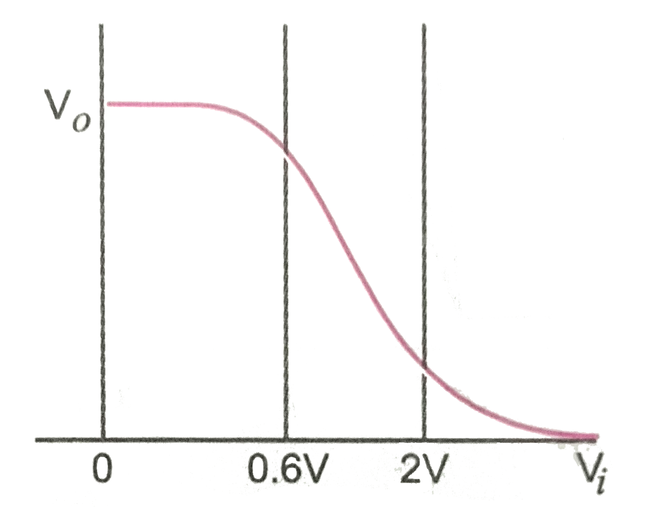
Fig.shows that transfer characteristics of a base biased CE transistor. Which of the following statements are true?

A
At Vi=0.4V, transistor is in active state
B
At Vi=1V, it can be used as an amplifier
C
At Vi=0.5V, it can be used as a switch turned off
D
At Vi=2.5V, can be used as a switch turned on
Video Solution
Text Solution
The correct Answer is:B, C, D
From the given transfer characteristics of a base biased common emitter transistor, we note that.
(i) When V1=0.4V, there is no collection current. The transistor circuit is in active state and is used as an amplifier,
(ii) When V1=1V (This is in between 0.6 V to 2V), the transistor circuit is in active state and is used as an amplifier,
(iii) When V1=0.5V, there is no collector currect. The transistor is in cut off state. The transistor circuit can be used as a switch turned off.
(iv) When V1=2.5V, the collector current becomes maximum and transistor is in saturation state and can used as switch turned on state.
|
Topper's Solved these Questions
Similar Questions
Knowledge Check
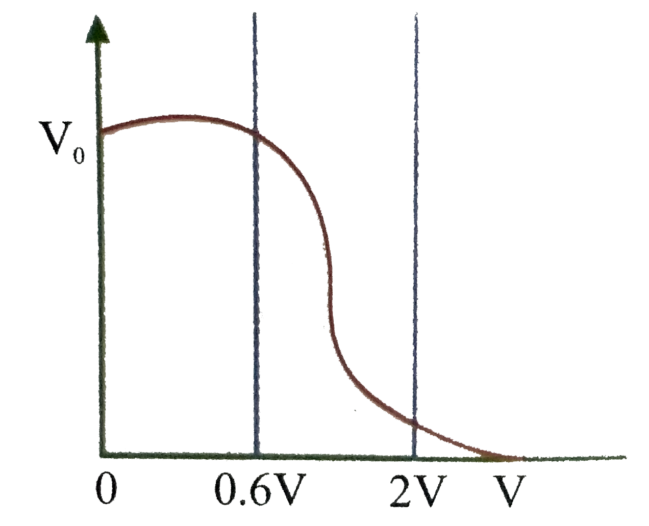
Figure shows the transfer characteristics of a base biased CE transistor. Which of the following statements are true ?

(A) At V1=0.14V transistors is in active state
(B) At V1=1V it can be used as an amplifier
(C) At V1=0.5V, it can be used as a switch turned off
(D) At V1=2.5V, it can be used as switch turned onAA,B,CBB,C,DCA,C,DDA,B,DThe transfer characteristics of a base biased common in the figure. Which of the following statements are true?
 AAt Vi=1V, it can be used as an amplifier.BAt Vi=0.5V, it can be used as a switch turned off.CAt Vi=2.5V, it can be used as a switch turned on.DAll of these
For transistor action, which of the following statements are correct ?
A(a) Base , emitter and collector regions should have similar size and doping concentrationsB(b) The base region must be very thin and lightly dopedC( c) The emitter junction is forward biased and collector junction is reverse biasedD(d) Both the emitter junction as well as the collector junction are forward biased
For transistor action, which of the following statements are correct ?
View SolutionWhich of the following is forward biased?
View SolutionWhich of the following is forward biased?
View SolutionThe transfer characteristics of a base biased transistor has the operation regions, namely, cutoff, active region and saturation region. For using the transistor as an amplifier it has to operate in the
View SolutionThe transfer characteristics of a base biased transistor has the operation regions, namely, cutoff, active region and saturation region. For using the transistor as an amplifier it has to operate in the
View Solution

