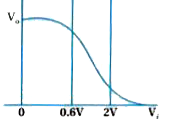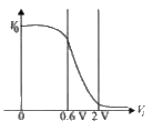
Figure shows the transfer characteristics of a base biased CE transistor. Which of the following statements are true? Solution in Gujrati
At Vi=0.4V, transistor is in active state.
At Vi=1V, it can be used as an amplifier.
At Vi=0.5V, it can be used as a switch turned off.
At Vi=2.5V, it can be used as a switch turned on.
The correct Answer is:B, C, D
A seen in the graph, active region of given transistor is from 0.6V to 2V. Hence when Vi=1V (inside active region), given transistor can be used as an amplifier. Thus, option (B) is correct.
For Vi=0.5V,IC≈0⇒ transistor will be in cut off state and so it will act like "off" condition of switch. Hence, option (C ) is correct.
For Vi=2.5V,IC becomes maximum and so transistor comes in saturation state and so it cna be used as a switch in "on" condition of switch. Hence, option (D) is also correct.
Topper's Solved these Questions
- SEMICONDUCTOR ELECTRONICS : MATERIALS, DEVICES AND SIMPLE CIRCUITS BOOK - KUMAR PRAKASHANCHAPTER - SEMICONDUCTOR ELECTRONICS : MATERIALS, DEVICES AND SIMPLE CIRCUITS EXERCISE - Section-C: NCERT Exemplar Solution (Very Short Answer Type Questions)
6 Videos
- SEMICONDUCTOR ELECTRONICS : MATERIALS, DEVICES AND SIMPLE CIRCUITS BOOK - KUMAR PRAKASHANCHAPTER - SEMICONDUCTOR ELECTRONICS : MATERIALS, DEVICES AND SIMPLE CIRCUITS EXERCISE - Section-C: NCERT Exemplar Solution (Short Answer Type Questions)
8 Videos
- SEMICONDUCTOR ELECTRONICS : MATERIALS, DEVICES AND SIMPLE CIRCUITS BOOK - KUMAR PRAKASHANCHAPTER - SEMICONDUCTOR ELECTRONICS : MATERIALS, DEVICES AND SIMPLE CIRCUITS EXERCISE - Section-C: NCERT Exemplar Solution (Multiple Choice Qustion (MCQs) )
8 Videos
- SAMPLE QUESTION PAPER BOOK - KUMAR PRAKASHANCHAPTER - SAMPLE QUESTION PAPER EXERCISE - PART-B SECTION-C
5 Videos
- WAVE OPTICSBOOK - KUMAR PRAKASHANCHAPTER - WAVE OPTICSEXERCISE - SECTION-D (MULTIPLCE CHOICE QUESTIONS (MCQS)) (MCQS FROM DARPAN BASED ON TEXTBOOK)
239 Videos
Similar Questions
Why are elemental dopants for Silicon on Germanium usually chosen from group XIII on group XV ?
View Solution
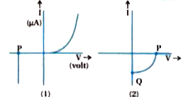
(i) Name the type of a diode whose characteristics are shown in figure (1) and figure (2).
(ii) What does the point P in figure (1) represent?
(iii) What does the points P and Q in figure (2) represent?
View SolutionThe conductivity of a semiconductor increases with increase in temperature because
View SolutionTwo charges –q and +q are located at points (0, 0, –a) and (0, 0, a), respectively.
(a) What is the electrostatic potential at the points (0, 0, z) and (x, y, 0) ?
(b) Obtain the dependence of potential on the distance r of a point from the origin when r/a>>1 .
(c) How much work is done in moving a small test charge from the point (5,0,0) to (–7,0,0) along the x-axis? Does the answer change if the path of the test charge between the same points is not along the x-axis?
View SolutionAccording to particle theory of light what is the velocity of light in a dense medium, compared to that in rare medium ?
View SolutionConsider an n-p-n transistor with its base - emitter junction forward biased and collector base junction reverse biased . Which of the following statements are true?
View SolutionDraw the transfer characteristic curve of a base biased transistor in CE configuration. Explain clearly how the active region of the Vo versus Vi curve in a transistor is used as an amplifier.
View SolutionFig.shows that transfer characteristics of a base biased CE transistor. Which of the following statements are true?
View SolutionConsider an n-p-n transistor with its base -emitter junction forward biased and collector -base junction reverse biased. Which of the following statements are true ?
View SolutionCE विधा में आधार बायसित ट्रांजिस्टर के लिए अंतरण ( Transfer ) अभिलाक्षणिक खींचिए | स्पष्ष्ट कीजिए की V0 के विरूद्ध Vi वक्र के सक्रिय क्षेत्र में ट्रांजिस्टर एक प्रवर्धक के रूप में किस प्रकार उपयोग में लाया जाता है ?
View SolutionDraw the transfer characteristic curve of a base biased transistor in CE configuration. Explain clearly how the active region of the V_0 versus V_F curve in a transistor is used as an amplifier.
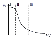
View Solutionकिसी भी आधार बायसित ट्राँजिस्टर के लिये CE विन्यास में अन्तरण अभिलक्षण [निर्गत वोल्टता (V0) तथा निवेश वोल्टता (Vi) के बीच ] आरेख में दर्शाया गया है। ट्रांजिस्टर का स्विच के रूप में उपयोग करने के लिये, इस का उपयोग किया जात है।

View SolutionConsider an n-p-n transistor with its base - emitter junction forward biased and collector base junction reverse biased . Which of the following statements are true?
View SolutionFig.shows that transfer characteristics of a base biased CE transistor. Which of the following statements are true?
View SolutionThe transfer characteristics of a base biased common in the figure. Which of the following statements are true?

View Solution
