How would you set up a circuit to obtain NOT gate using a transistor?Solution in Punjabi
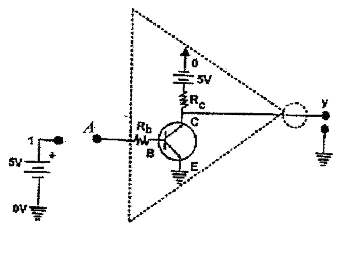
The NOT gate can be realised by making use of transistor . The base (B) of the transistor is connected to A through a resistor Rb while the emitter (E ) is earthed . The collector is earthed through a resistor RC and a 5V battery in following two case :
(a) A = (0) . The base of the transistor also gets earthed . Therefore , base - emitter junction in not forward biased . Since the base current in zero , the collector current is also zero. The transistor is said to be in cut - off mode . The output y will be equal to the voltage of battery connected to collector i.e., 5V. In other words , When A = 0 , y = 1 .

(b) A = 1 . The base- emitter junction gets forwards biased and it leads to a large collector current . The transistor is said to have gone to saturation . The voltage drop across the resistor Rc in just equal to 5 V and the output y is very nearly 0.
Topper's Solved these Questions
- BOOK - BETTER CHOICE PUBLICATIONCHAPTER - DIGITAL ELECTRONICS EXERCISE - LONG ANSWERS TYPE QUESTIONS3videos
DIGITAL ELECTRONICS
- BOOK - BETTER CHOICE PUBLICATIONCHAPTER - DIGITAL ELECTRONICS EXERCISE - LONG ANSWERS TYPE QUESTIONS3videos
DIGITAL ELECTRONICS
- BOOK - BETTER CHOICE PUBLICATIONCHAPTER - DIFFRACTION OF LIGHTEXERCISE - Numberical Problem1videos
DIFFRACTION OF LIGHT
- BOOK - BETTER CHOICE PUBLICATIONCHAPTER - DIPERSION OF LIGHTEXERCISE - MOST EXPECTED QUESTIONS5videos
DIPERSION OF LIGHT
Similar Questions
Draw the logic symbol of NOT gate. Write. its truth table. Explain, how this gate can be realized in actual practice by using transistor
01:54View SolutionDraw the logic symbol of NOT gate. Write. its truth table. Explain, how this gate can be realized in actual practice by using transistor
03:11View SolutionA concave lens of focal length 15cm forms an image 10 cm from the lens. How far is the object placed from the lens? Draw ray diagram.
04:41View SolutionWhat do you mean by dispersion of light?
01:54View SolutionHow would you set up a circuit to obtain NOT gate using a transistor?
03:32View SolutionExplain with the help of a diagram, how you would construct a NOT gate by using an n-p-n transistor.
04:12View SolutionHow would you construct the basic gates by using either
NOR gate or (ii) NAND gate?02:43View SolutionHow would you construct a NOT gate by using a NOR gate.
04:16View SolutionHow would you construct an AND gate by using minimum number of OR and NOT gate.
04:52View SolutionHow would you construct an OR gate by using minimum number of AND and NOT gates.
03:29View SolutionHow would you construct an AND gate by using more than one NAND gate?
02:30View SolutionHow would you set up a circuit to obtain NOT gate using a transistor?
01:42View SolutionHow would you set up a circuit to obtain NOT gate using a transistor?
09:27View SolutionWrite the truth table of NOR gate.Draw the symbol of NOR gate. Draw a circuit to obtain OR gate using NOR gate only.
View SolutionHow would you set up a circuit to obtain NOT gate using a transistor?
01:58View SolutionUsing several NAND gates, how can you obtain an AND gate ? Draw a labelled diagram in support of your answer.
03:30View Solution

