In junction, the barrier potential offerse resistance to
The resistance of intrinsic of semiconductor decrease with increases of temperature
Doping pure with interval impurities give -type semiconductor
Only free electrons in -type semiconductor are holes
Only holes in region
The correct Answer is:A
Step by step video, text & image solution for In P-N junction, the barrier potential offerse resistance to by Physics experts to help you in doubts & scoring excellent marks in Class 12 exams.
Updated on:21/07/2023Topper's Solved these Questions
- SEMICONDUCTOR ELECTRONICSBOOK - A2ZCHAPTER - SEMICONDUCTOR ELECTRONICSEXERCISE - Diode In Circuits
40 Videos
- SEMICONDUCTOR ELECTRONICSBOOK - A2ZCHAPTER - SEMICONDUCTOR ELECTRONICSEXERCISE - Junction Transistor
47 Videos
- SEMICONDUCTOR ELECTRONICSBOOK - A2ZCHAPTER - SEMICONDUCTOR ELECTRONICSEXERCISE - Classification Of Metals
64 Videos
- NUCLEAR PHYSICSBOOK - A2ZCHAPTER - NUCLEAR PHYSICSEXERCISE - Section D - Chapter End Test
29 Videos
- SOURCE AND EFFECT OF MAGNETIC FIELDBOOK - A2ZCHAPTER - SOURCE AND EFFECT OF MAGNETIC FIELDEXERCISE - Section D - Chapter End Test
30 Videos
Similar Questions
Knowledge Check
In a p-n junction , the barrier potential offers resistance to
AFree electrons in n-side and holes in p-sideBfree electrons in p-side and holes in n-sideCOnly free electrons in n-sideDOnly holes in p-sideIn a p−n junction diode, the barrier potential opposes diffusion of
Afree electrons from n- regionBholes from p- regionCmajority charge carriers from both the regionsDminority charge carriers from both the regionsBarrier potential of Ga-As-P LED is
A0.7 VB1.0 VC0.3 VD1.5 V
In a p-n junction,a potential barrier of 250 mev exsists across the junction.A hole with a kimetic energy of 300 meV approaches the junction. Find the kinetic energy of the hole when it crosses the junction if the hole approached the junction (a)from the p-side and (b)from the n-side.
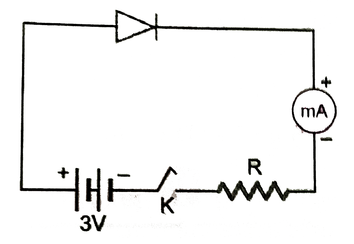
View SolutionWhen a p-type semiconductor is brought into a close contact with n-type semiconductor, we get a p-n junction with a barrier potential 0.4V and the width of depletion region is 4.0×10⁻⁷m. this p-n junction is forwaed biased with a battery of voltage 3V adn negligible internal resistance, in series with a resistance of resistance R, ideal milliammeter and key K as shown in Fig.

The intensity of the electric field in the depletion region when p-n junction is unbiased is
View SolutionWhen a p-type semiconductor is brought into a close contact with n-type semiconductor, we get a p-n junction with a barrier potential 0.4V and the width of depletion region is 4.0×10⁻⁷m. this p-n junction is forwaed biased with a battery of voltage 3V adn negligible internal resistance, in series with a resistance of resistance R, ideal milliammeter and key K as shown in Fig.

The resistance of resistor R is
View SolutionWhen a p-type semiconductor is brought into a close contact with n-type semiconductor, we get a p-n junction with a barrier potential 0.4V and the width of depletion region is 4.0×10⁻⁷m. this p-n junction is forwaed biased with a battery of voltage 3V adn negligible internal resistance, in series with a resistance of resistance R, ideal milliammeter with reading 20 mA and key K as shown in Fig.

The resistance of resistor R is
View Solution
