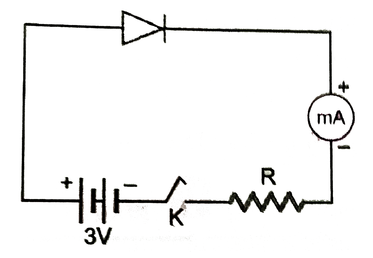
When a p-type semiconductor is brought into a close contact with n-type semiconductor, we get a p-n junction with a barrier potential 0.4V and the width of depletion region is 4.0×10⁻⁷m. this p-n junction is forwaed biased with a battery of voltage 3V adn negligible internal resistance, in series with a resistance of resistance R, ideal milliammeter with reading 20 mA and key K as shown in Fig.

The resistance of resistor R is
1.39×10⁵ms−1
2.78×10⁵ms−1
1.39×10⁶ms−1
2.78×10⁶ms−1
The correct Answer is:A
Let v1 be the speed of electron when enters the depletion region and v2 is the speed when it comes out of depletion layer. According to principle of conservation of total energy,
K.E. of the incident electron =workdone against potential barrier +K.E. of the emerging electron.
i.e. 12mv21=eV+12mv22
or 12×(9.1×10−31)×(4×105)2
=(1.6×10−19×(0.4)+12×9.1×10−31×v22
on solving, we get, v2=1.39×10⁵ms−1
Topper's Solved these Questions
- BOOK - PRADEEPCHAPTER - ELECTRONIC DEVICESEXERCISE - INTEGER TYPE QUESTION2videos
ELECTRONIC DEVICES
- BOOK - PRADEEPCHAPTER - ELECTRONIC DEVICESEXERCISE - MULTIPLE CHOICE QUESTIONS2videos
ELECTRONIC DEVICES
- BOOK - PRADEEPCHAPTER - ELECTRONIC DEVICESEXERCISE - PROBLEMS FOR PRACTICE7videos
ELECTRONIC DEVICES
- BOOK - PRADEEPCHAPTER - ELECTROMAGNETIC WAVESEXERCISE - II Focus multiple choice question5videos
ELECTROMAGNETIC WAVES
- BOOK - PRADEEPCHAPTER - ELECTROSTATICSEXERCISE - ASSERTION-REASON TYPE QUESTIONS2videos
ELECTROSTATICS
Similar Questions
Knowledge Check
- Question 1 - Select One
When a p-type semiconductor is brought into a close contact with n-type semiconductor, we get a p-n junction with a barrier potential 0.4V and the width of depletion region is 4.0×10⁻⁷m. this p-n junction is forwaed biased with a battery of voltage 3V adn negligible internal resistance, in series with a resistance of resistance R, ideal milliammeter and key K as shown in Fig.

The resistance of resistor R isA150ΩB300ΩC130ΩD180Ω - Question 2 - Select One
When a p-type semiconductor is brought into a close contact with n-type semiconductor, we get a p-n junction with a barrier potential 0.4V and the width of depletion region is 4.0×10⁻⁷m. this p-n junction is forwaed biased with a battery of voltage 3V adn negligible internal resistance, in series with a resistance of resistance R, ideal milliammeter with reading 20 mA and key K as shown in Fig.

The resistance of resistor R isA0.060 WB0.052 WC0.008 WD0.048 W - Question 3 - Select One
When a p-type semiconductor is brought into a close contact with n-type semiconductor, we get a p-n junction with a barrier potential 0.4V and the width of depletion region is 4.0×10⁻⁷m. this p-n junction is forwaed biased with a battery of voltage 3V adn negligible internal resistance, in series with a resistance of resistance R, ideal milliammeter and key K as shown in Fig.

The intensity of the electric field in the depletion region when p-n junction is unbiased isA0.5×106Vm−1B1.0×106Vm−1C2.0×106Vm−1D1.5×106Vm−1
Semiconductor || P-N junction
View SolutionWhen a p-type semiconductor is brought into a close contact with n-type semiconductor, we get a p-n junction with a barrier potential 0.4V and the width of depletion region is 4.0×10⁻⁷m. this p-n junction is forwaed biased with a battery of voltage 3V adn negligible internal resistance, in series with a resistance of resistance R, ideal milliammeter with reading 20 mA and key K as shown in Fig.

The resistance of resistor R isView SolutionWhen n and p-type semiconductors are allowed to come into contact
View SolutionIn a p-n junction , the barrier potential offers resistance to
View SolutionIn P−N junction, the barrier potential offerse resistance to
View Solution

