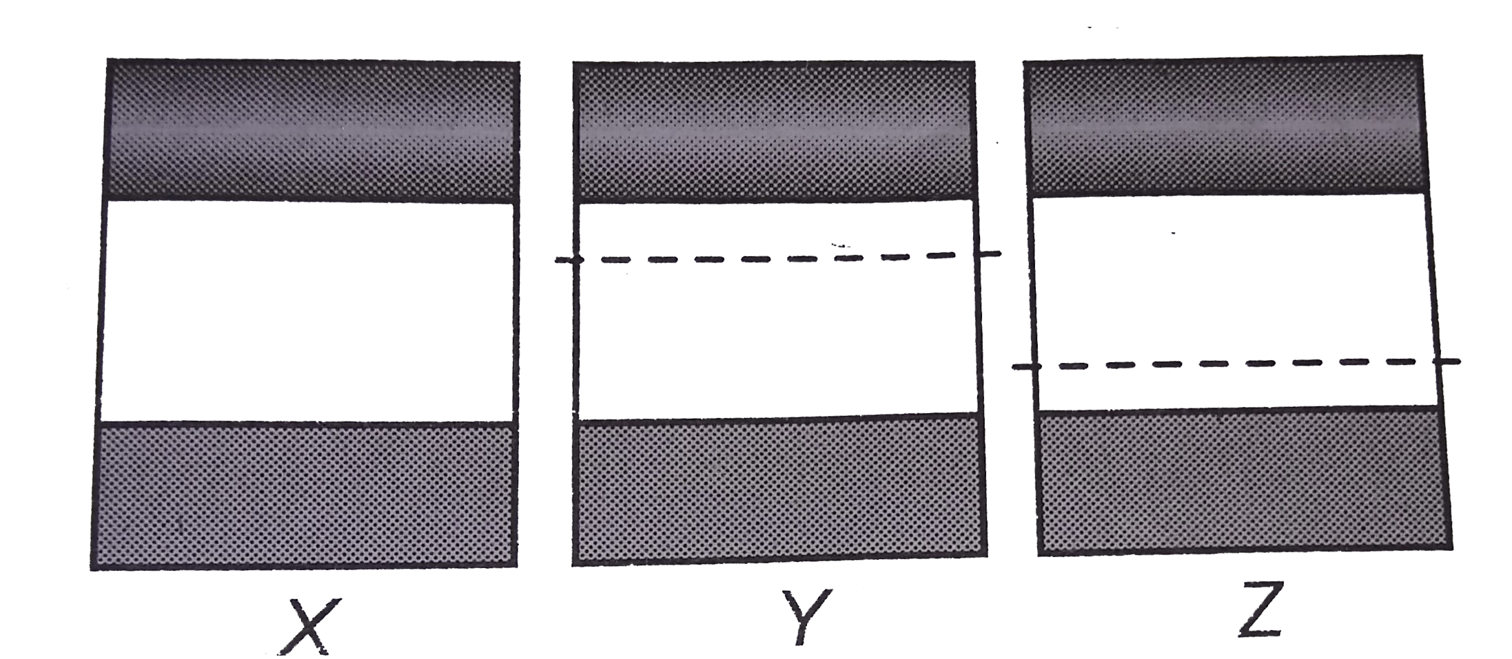
In the energy band diagram of a material shown below, the open circles and filled circles denote holes and electrons respectively. The material is a/an
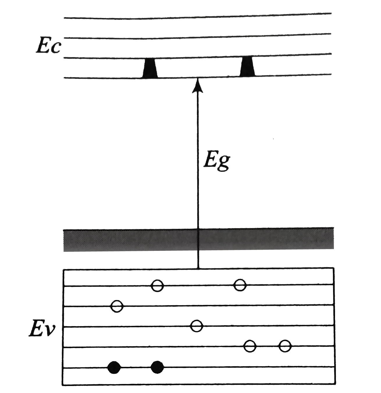
p-type semiconductor
insulator
metal
n-type semiconductor
The correct Answer is:A
Step by step video, text & image solution for In the energy band diagram of a material shown below, the open circles and filled circles denote holes and electrons respectively. The material is a/an by Physics experts to help you in doubts & scoring excellent marks in Class 12 exams.
Updated on:21/07/2023Topper's Solved these Questions
Similar Questions
Knowledge Check
In a semiconducting material, the mobilities of electrons and holes are μe and μh respectively. Then
Aμe<μhBμe=μhCμe<μhDμe>0 but μh<1Which of the energy band diagrams shown in the figure corresponds to that of a semiconductor?
A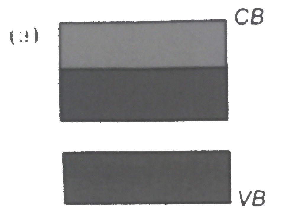 B
B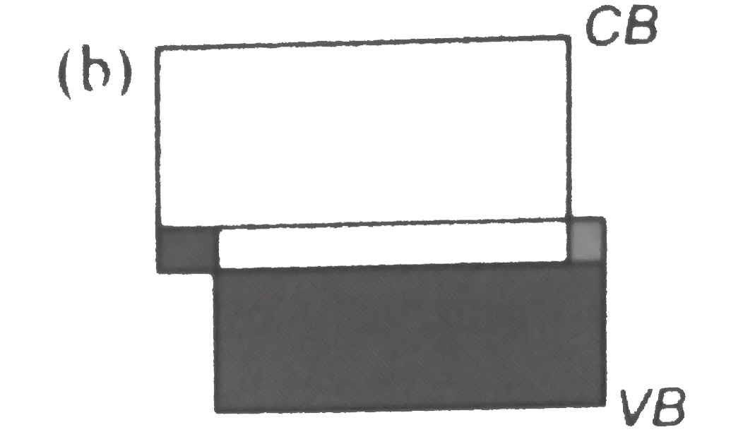 C
C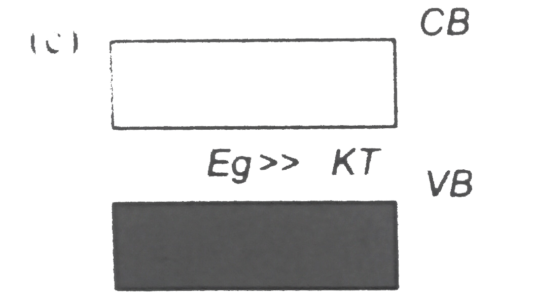 D
D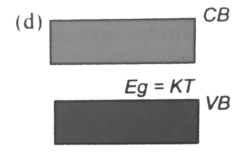
Assertion: If there is some gap between the conduction band and the valence band, electrons in the valence band all remain bound and no free electrons are available in the conduction band. Then the material is an insulator.
Reason: Resistance of insulators is very lowAIf both assertion and reason are true and reason is the correct explanation of assertion.BIf both assertion and reason are true not but reason is not the correct explanation of assertion.CIf assertion is true but reason is falseDIf both assertion and reason are false.
Draw the "energy bands" diagram for a (i) pure semiconductor (ii) insulator. How does the energy band, foe a pure semiconductor, get affected when this semiconductor is doped with an acceptor impurity donor impurity? Hence discuss why the 'holes' and the 'electrons' respectively, become the 'majority charge carriers' in these two cases.
View SolutionIf p is the resistivity of a material, and n is the number density of free electrons in it, the mean time between collisions between electrons in the material is given by: (m denotes the mass of an electron, and e denotes the charge on an electron)
View SolutionFor the circle shown below, find the length (in cm.) of the largest chord of the circle.
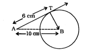
View SolutionStudy the following diagram consisting of a circle, a rectangle and a triangle and answer the question given below it.
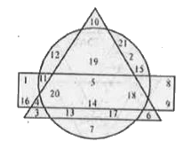
If the circle is called 'rectangle rectangle is called triangle' and triangle is called 'circle', which number is only in the triangle but not in other two diagrams?
View SolutionThe energy band diagrams for three semiconductor samples of silicon are as shown. We can then assert that
View Solution


