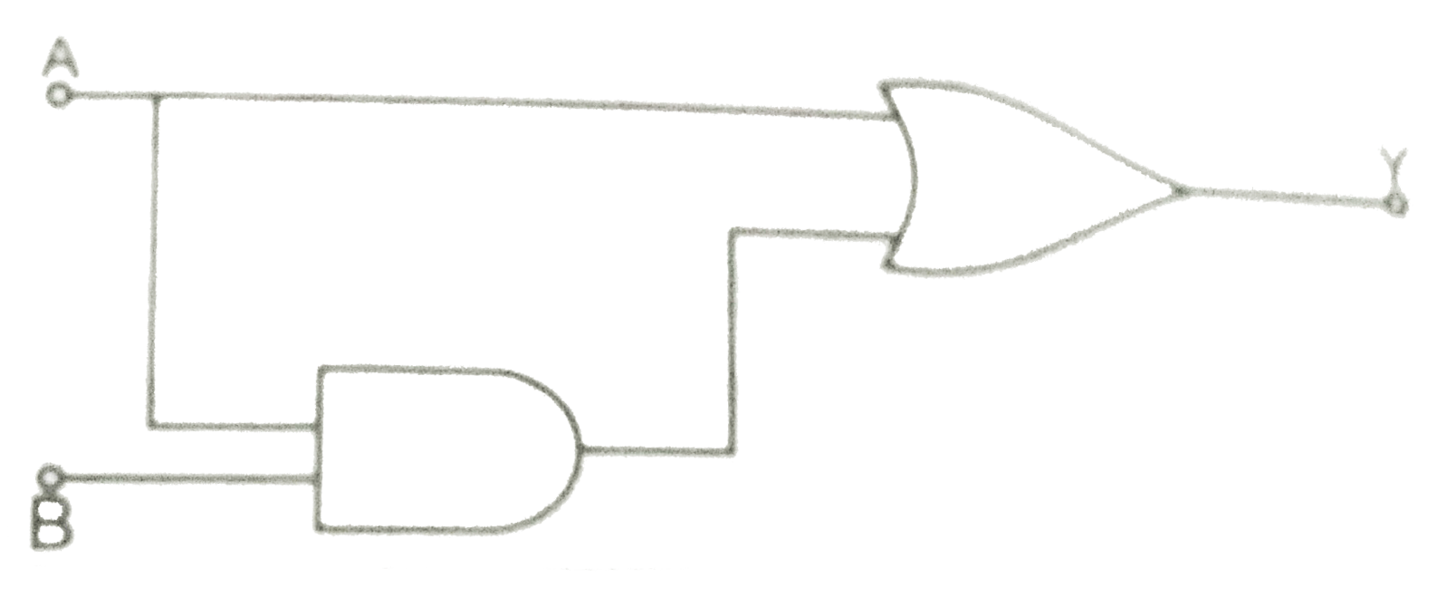
In the following circuit, the output Y for all possible inputs A and B is expressed by the truth table:

A
∣∣ ∣ ∣ ∣ ∣ ∣∣ABY000010100111∣∣ ∣ ∣ ∣ ∣ ∣∣
B
∣∣ ∣ ∣ ∣ ∣ ∣∣ABY001011101110∣∣ ∣ ∣ ∣ ∣ ∣∣
C
∣∣ ∣ ∣ ∣ ∣ ∣∣ABY001010100110∣∣ ∣ ∣ ∣ ∣ ∣∣
D
∣∣ ∣ ∣ ∣ ∣ ∣∣ABY000011101111∣∣ ∣ ∣ ∣ ∣ ∣∣
Video Solution
Text Solution
The correct Answer is:D
Gates−I and II are NOR gates. We can simplify the gate circuit as

Here, gates I and II are NOR gates. The output ¯¯¯¯¯¯¯¯¯¯¯A+Bof gate I will be appeared as input of gate II. The final output is Y=¯¯¯¯¯¯¯¯¯¯¯¯¯¯¯¯¯¯¯¯¯¯A+B=A+B
This is the Boolean expression of OR gate whose truth table is given below
∣∣
∣
∣
∣
∣
∣∣ABY000011101111∣∣
∣
∣
∣
∣
∣∣
|
Topper's Solved these Questions
- SEMICONDUCTOR ELECTRONICSBOOK - A2ZCHAPTER - SEMICONDUCTOR ELECTRONICSEXERCISE - AIIMS Questions
38 Videos
- SEMICONDUCTOR ELECTRONICSBOOK - A2ZCHAPTER - SEMICONDUCTOR ELECTRONICSEXERCISE - Assertion Reason
18 Videos
- SEMICONDUCTOR ELECTRONICSBOOK - A2ZCHAPTER - SEMICONDUCTOR ELECTRONICSEXERCISE - Section B - Assertion Reasoning
22 Videos
- NUCLEAR PHYSICSBOOK - A2ZCHAPTER - NUCLEAR PHYSICSEXERCISE - Section D - Chapter End Test
29 Videos
- SOURCE AND EFFECT OF MAGNETIC FIELDBOOK - A2ZCHAPTER - SOURCE AND EFFECT OF MAGNETIC FIELDEXERCISE - Section D - Chapter End Test
30 Videos
Similar Questions
Knowledge Check
In the following circuit the output Y becomes zero for the inputs
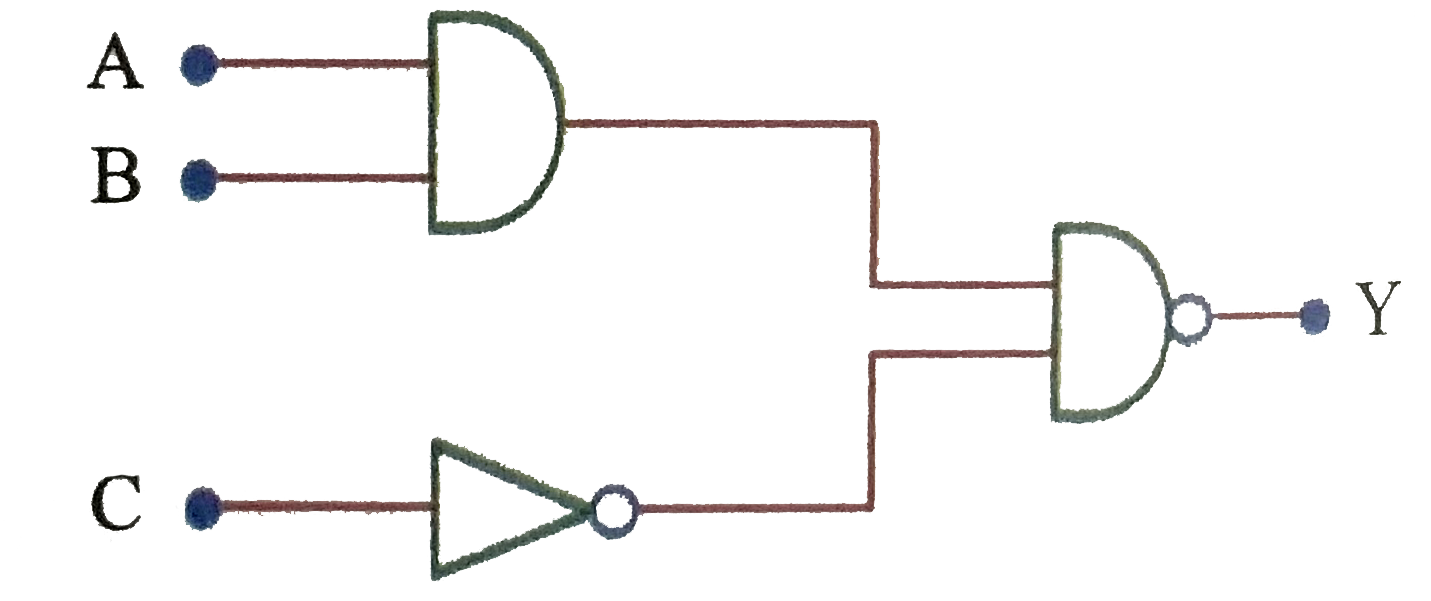 .AA=1,B=0,C=0BA=0,B=1,C=1CA=0,B=0,C=0DA=1,B=1,C=0
In AND gate, the output Y is 1 when the inputs A and B are:
AA=1, B=0BA=1, B=1CA=0, B=0DA=0, B=1In the circuit Fig. the output y becomes zero for the inputs
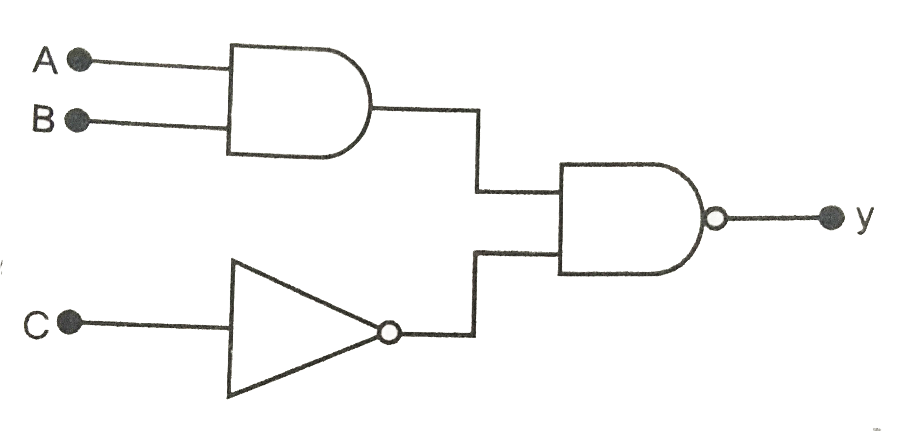 AA=1,B=0,C=0BA=0,B=1,C=1CA=0,B=0,C=0DA=1,B=1,C=0
The Boolean expression of the output Y of the inputs A and B for the circuit shown in the fig.
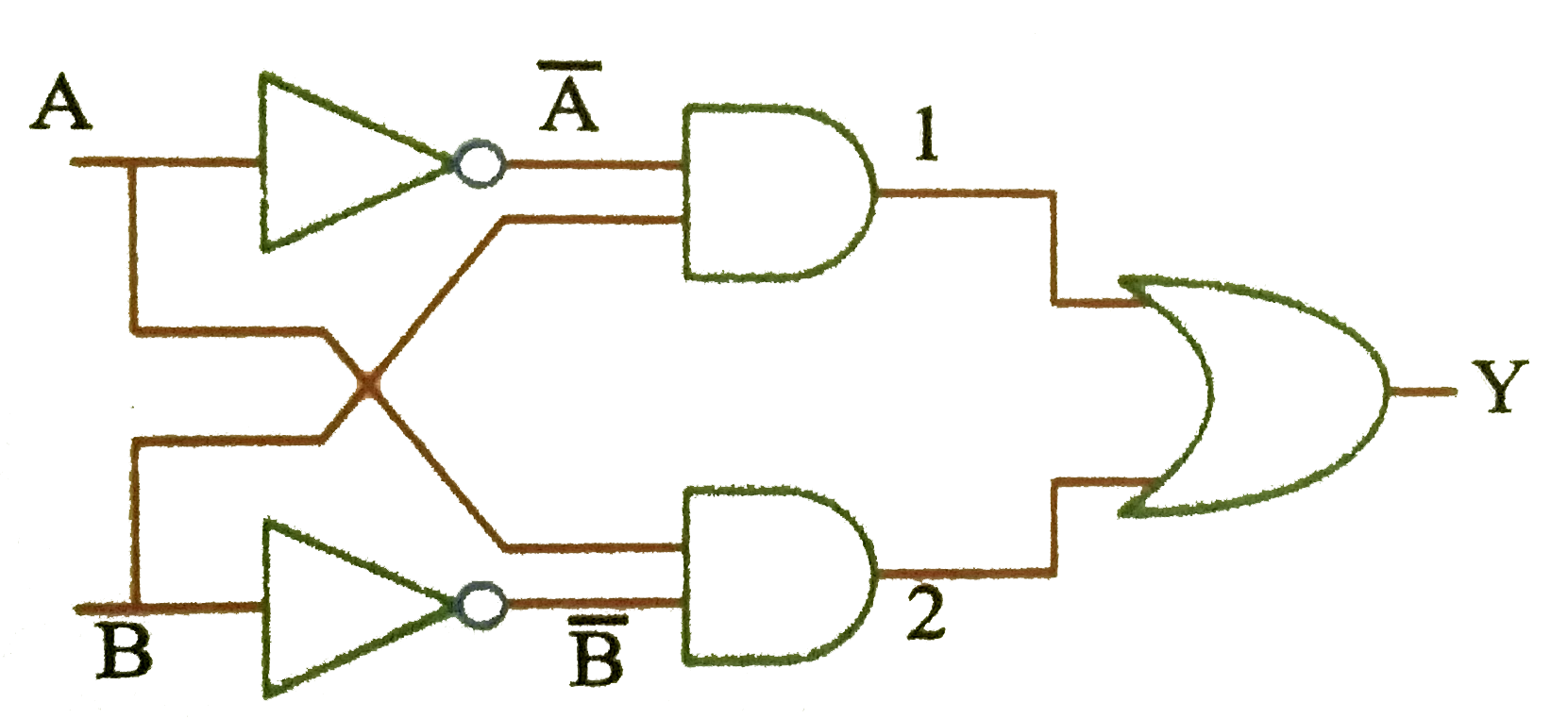 .
.
View SolutionIn the logic circuit shown in the figure, if input A and B are 0 to 1 respectively, the output at Y would be ‘x’
The value of x is _______

View SolutionWhich of the following is the truth table for the circuit below ?

View SolutionThe Boolean expression of the output Y of the inputs A and B for the circuit shown in the fig.
 .
.
View SolutionIf the Output of two NAND gates is given to input of a NAND gate. Then the truth table will be of
View Solution

