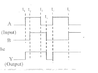
Justify the output waveform (Y) of the OR gate for the following inputs A and B given in the figure below .Solution in Tamil
At t<t1, A=0,B=0, Hence Y = 0
For t1 to t2, A=1,B=0 , Hence Y = 1
For t2 to t3, A=1,B=1, Hence Y = 1
For t3 to t4, A=0,B=1 , Hence Y = 1
For t4 to t5, A=0,B=0, Hence Y = 0
For t5 to t6, A=1,B=0 , Hence Y = 1
For t>t6, A=0,B=1 , Hence Y = 1
Therefore the waveform Y will be as shown in the figure .

Topper's Solved these Questions
- SEMICONDUCTOR ELECTRONICS : MATERIALS , DEVICES AND SIMPLE CIRCUITS BOOK - NEW JOYTHI PUBLICATIONCHAPTER - SEMICONDUCTOR ELECTRONICS : MATERIALS , DEVICES AND SIMPLE CIRCUITS EXERCISE - SOLUTION TO EXERCISES FROM NCERT TEXT
17 Videos
- SEMICONDUCTOR ELECTRONICS : MATERIALS , DEVICES AND SIMPLE CIRCUITS BOOK - NEW JOYTHI PUBLICATIONCHAPTER - SEMICONDUCTOR ELECTRONICS : MATERIALS , DEVICES AND SIMPLE CIRCUITS EXERCISE - PRACTICE PROBLEMS FOR SELF ASSESSMENT
8 Videos
- RAY OPTICS AND OPTICAL INSTRUMENTS BOOK - NEW JOYTHI PUBLICATIONCHAPTER - RAY OPTICS AND OPTICAL INSTRUMENTS EXERCISE - COMPETITIVE EXAM CORNER
26 Videos
- WAVE OPTICSBOOK - NEW JOYTHI PUBLICATIONCHAPTER - WAVE OPTICSEXERCISE - COMPETITIVE EXAM CORNER
17 Videos
Similar Questions
In an n-type silicon , which of the following statements is true ?
View SolutionA semiconductor has the electron concentration 0.45×10¹²m−3 and hole concentration 5×1029m−3 . Find its conductivity . Given electron mobility = 0.135m2V−1s−1 and hole mobility = 0.048m2V−1s−1,e=1.6×10⁻¹⁹C
View SolutionA 100 W bulb produces an electric field of 2.9 V/m at a point 3m away. If the bulb is replaced by 400 W bulb without disturbing other conditions. Then the electric field produced at the same point is
View SolutionYoung's experiment is performed with light of wavelength 6000Å where in 16 frignes occupy a certain region on the screen. If 24 fringes occupy the same region with another light of wavelength λ then λ is
View SolutionThe following Fig. shows the input waveforms (A,B) and the output waveform (y) of a gate. Identify the gate and write its truth table.
View SolutionThe following figure shows a logic gate circuit with two inputs A and B and the output Y . The voltage waveforms of A,B and the output Y are as given
View SolutionThe following figure shows a logic gate circuit with two inputs A and B and the output Y. The voltage waveforms of A,B and Y are as given : The logic gate is
View SolutionShow the output waveform of OR gate for the following input waveforms of A and B

View Solutionshow the output waveform of AND gate for the following input waveforms of A and B.

View SolutionShow the output waveform of OR gate for the following input waveforms of A and B
View SolutionJustify the output waveform (Y) of the OR gate for the following inputs A and B given in
View SolutionJustify the output waveform (Y) of the OR gate for the following inputs A and B given in
View SolutionJustify the output waveform (Y) of the OR gate for the following inputs A and B given in
View SolutionJustify the output waveform (Y) of the OR gate for the following inputs A and B given in the figure below .
View SolutionJustify the output waveform (Y) of the OR gate for the following inputs A and B given in
View Solution
