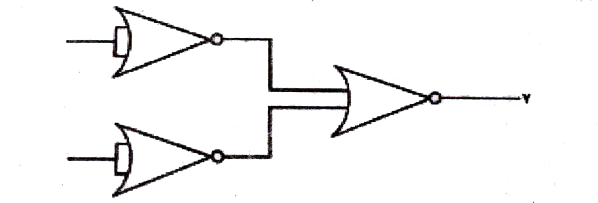
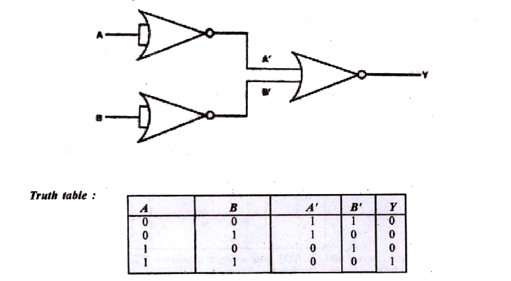
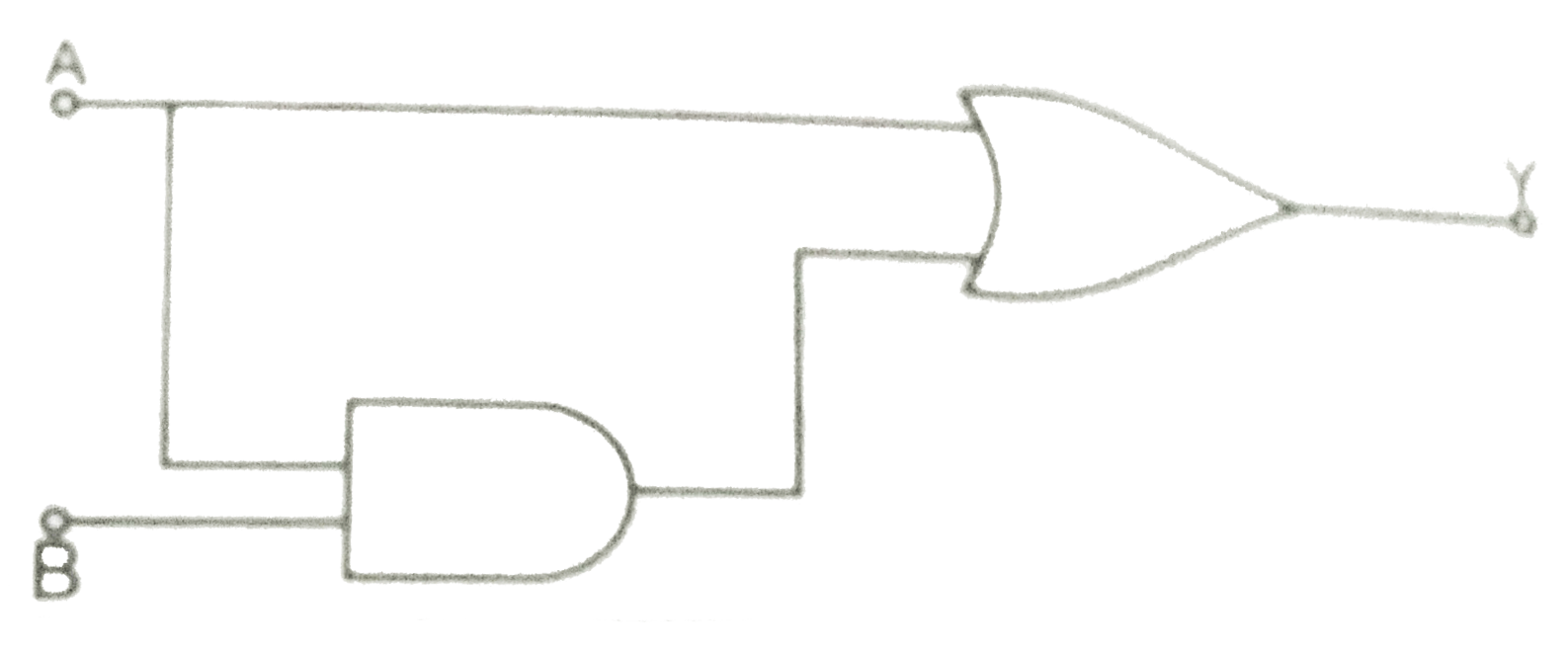
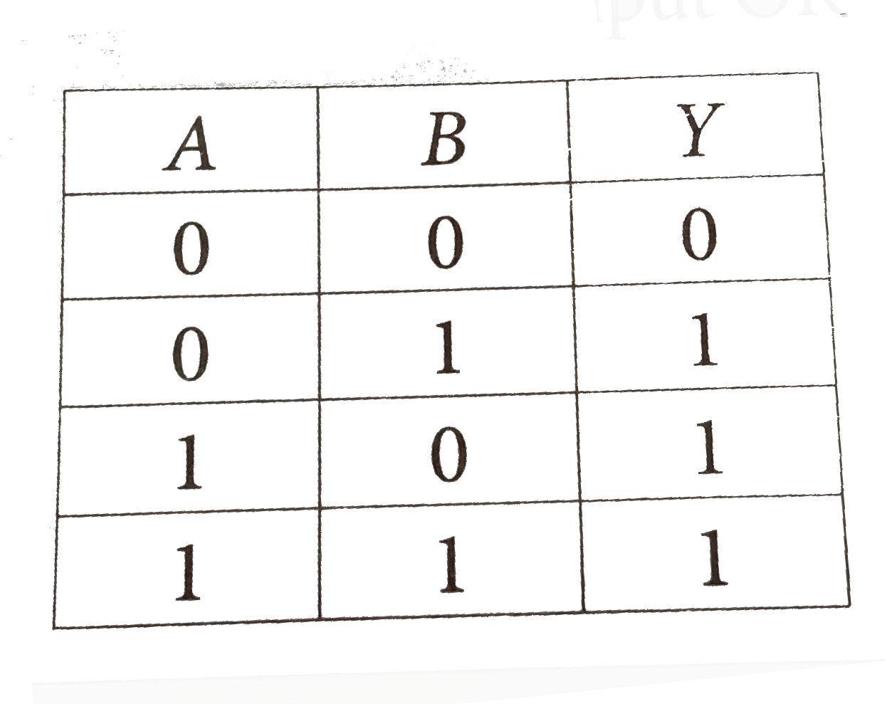
Make the truth table for all possible inputs of the following circuit .
 Solution in Punjabi

The given digital circuit behaves as an AND gate .
Topper's Solved these Questions
- BOOK - BETTER CHOICE PUBLICATIONCHAPTER - DIGITAL ELECTRONICS EXERCISE - LONG ANSWERS TYPE QUESTIONS3videos
DIGITAL ELECTRONICS
- BOOK - BETTER CHOICE PUBLICATIONCHAPTER - DIGITAL ELECTRONICS EXERCISE - LONG ANSWERS TYPE QUESTIONS3videos
DIGITAL ELECTRONICS
- BOOK - BETTER CHOICE PUBLICATIONCHAPTER - DIFFRACTION OF LIGHTEXERCISE - Numberical Problem1videos
DIFFRACTION OF LIGHT
- BOOK - BETTER CHOICE PUBLICATIONCHAPTER - DIPERSION OF LIGHTEXERCISE - MOST EXPECTED QUESTIONS5videos
DIPERSION OF LIGHT
Similar Questions
Draw the logic symbol of NOT gate. Write. its truth table. Explain, how this gate can be realized in actual practice by using transistor
01:58View SolutionDraw the logic symbol of NOT gate. Write. its truth table. Explain, how this gate can be realized in actual practice by using transistor
05:01View SolutionA concave lens of focal length 15cm forms an image 10 cm from the lens. How far is the object placed from the lens? Draw ray diagram.
02:18View SolutionWhat do you mean by dispersion of light?
03:18View SolutionIn the following circuit, the output Y for all possible inputs A and B is expressed by the truth table:
 02:08View Solution
Express by a truth table, the output Y for all possible input A and B in the following circuit Fig.
 View Solution
The output of a 2-inputs NAND gate is fed to a NOT gate. Write down the truth table for the output of the combination for all possible input of the combination for all possible inputs of A and B.
03:01View SolutionIdentify the logic gate equivalent to the circuit shown in the Fig.Draw the truth table for all possible values of inputs A and B.
03:59View SolutionAssertion: This circuit acts as OR Gate. Reason: Truth table for two input OR Gate is
03:07View SolutionFor the digital circuit given below, write the truth table showing outputs Y_1 and Y_2 for all possible inputs of A and B.
02:14View Solutionचित्र में प्रदर्शित परिपथ के लिये सभी सम्भव A और B निवेशीयों के लिये निर्गत Y को इनमें से किस सत्य सारणी द्वारा व्यक्त किया जा सकता है?
 01:18View Solution
Write down the truth table for output Y for all possible inputs A and B in the following circuit:
 02:30View Solution
Assertion:

This circuit acts as OR Gate.
Reason: Truth table for two input OR Gate is View Solution
In the following circuit, the output Y for all possible inputs A and B is expressed by the truth table:
 View Solution
Draw the circuit symbol and write the truth table of a two-input NAND gate.
View SolutionWrite down the truth table and circuit symbol of 3-input NOR gate.
View Solution

