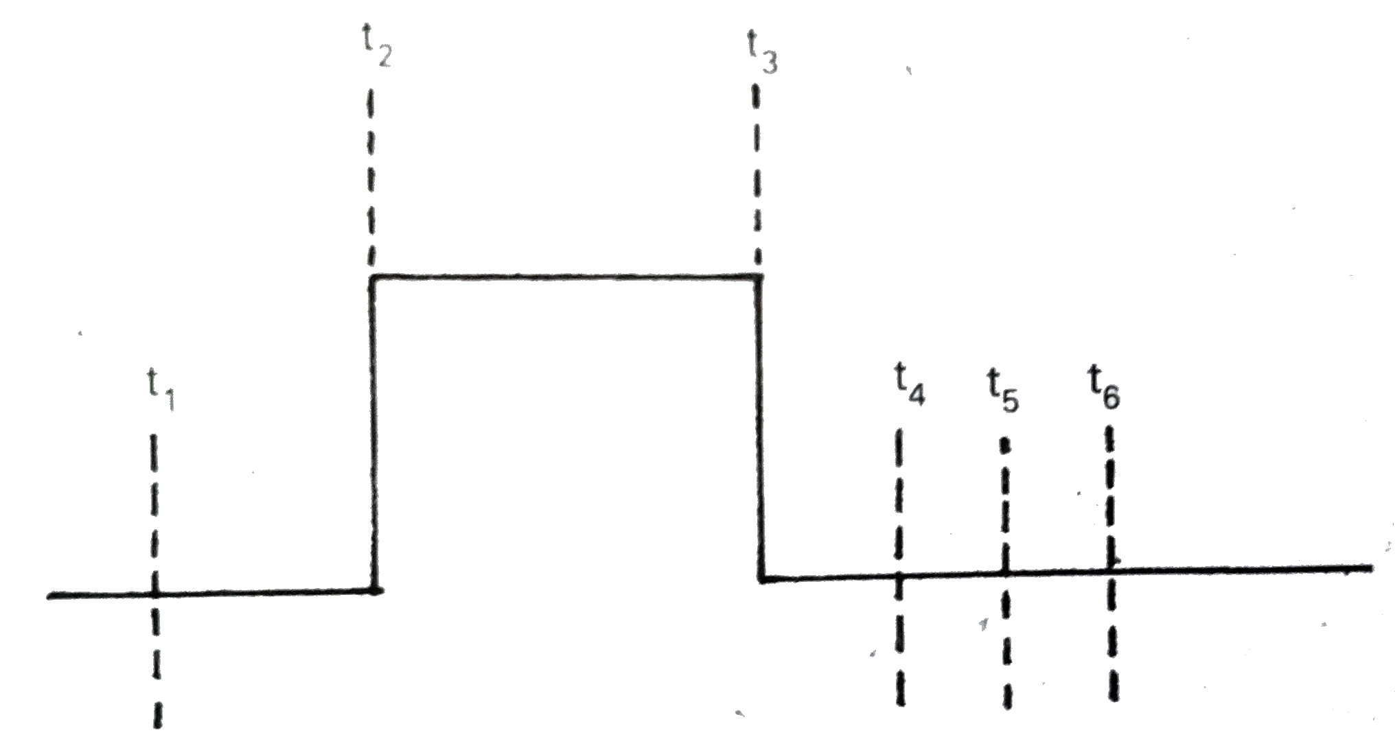
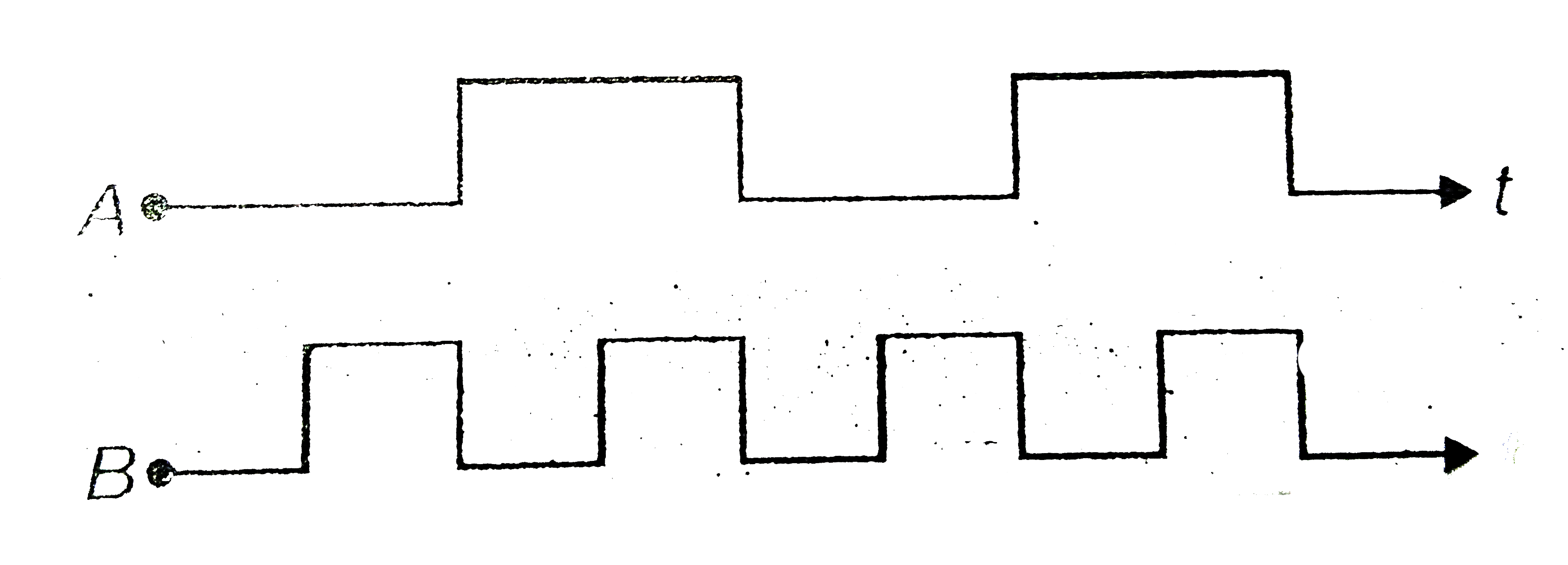
Take A and B input waveforms similar to that in Example .Sketch the output waveform obtained from AND gate.
For t≤t1,A=0,B=0,Hence Y=0
For t1 to t2,A=1,B=0, Hence Y =0
For t2 to t3,A=1,B=1, Hence Y=1
For t3 to t4,A=0,B=1, Hence Y=0
For t4 to t5,A=0,B=0, Hence Y=0
For t5to t6,A=1,B=0, Hence Y=0
For t>t6,A=0,B=1, Hence Y = 0
Based on the above, the output waveform for AND gate can be drawn as given below .
Topper's Solved these Questions
- BOOK - VIKRAM PUBLICATION ( ANDHRA PUBLICATION)CHAPTER - SEMICONDUCTOR ELECTRONICS : MATERIALS , DEVICES , AND SIMPLE CIRCUITS EXERCISE - PROBLEMS4videos
SEMICONDUCTOR ELECTRONICS : MATERIALS , DEVICES , AND SIMPLE CIRCUITS
- BOOK - VIKRAM PUBLICATION ( ANDHRA PUBLICATION)CHAPTER - SEMICONDUCTOR ELECTRONICS : MATERIALS , DEVICES , AND SIMPLE CIRCUITS EXERCISE - VERY SHORT ANSWER QUESTIONS14videos
SEMICONDUCTOR ELECTRONICS : MATERIALS , DEVICES , AND SIMPLE CIRCUITS
- BOOK - VIKRAM PUBLICATION ( ANDHRA PUBLICATION)CHAPTER - RAY OPTICAL AND INSTRUMENTSEXERCISE - TEXTUAL EXERCISES60videos
RAY OPTICAL AND INSTRUMENTS
- BOOK - VIKRAM PUBLICATION ( ANDHRA PUBLICATION)CHAPTER - TELANGANA MARCH-2019EXERCISE - SECTION -B5videos
TELANGANA MARCH-2019
Similar Questions
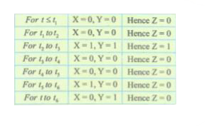
Take X and Y input waveforms. Sketch the output (Z) waveform abtained from AND gate as per the following conditions:
 View Solution
Write the output waveform for the gates
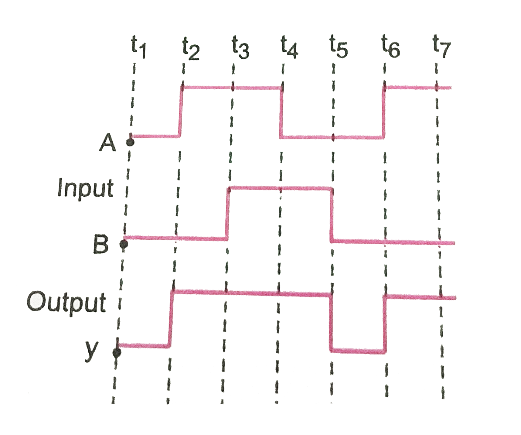
View SolutionThe Fig shown input waveforms A and B to a logic gate. Draw the output waveform for an OR gate. Write the truth table for this logic gate and draw its logic symbol.
 View Solution
The Fig shown input waveforms A and B to a logic gate. Draw the output waveform for an OR gate. Write the truth table for this logic gate and draw its logic symbol.
 View Solution
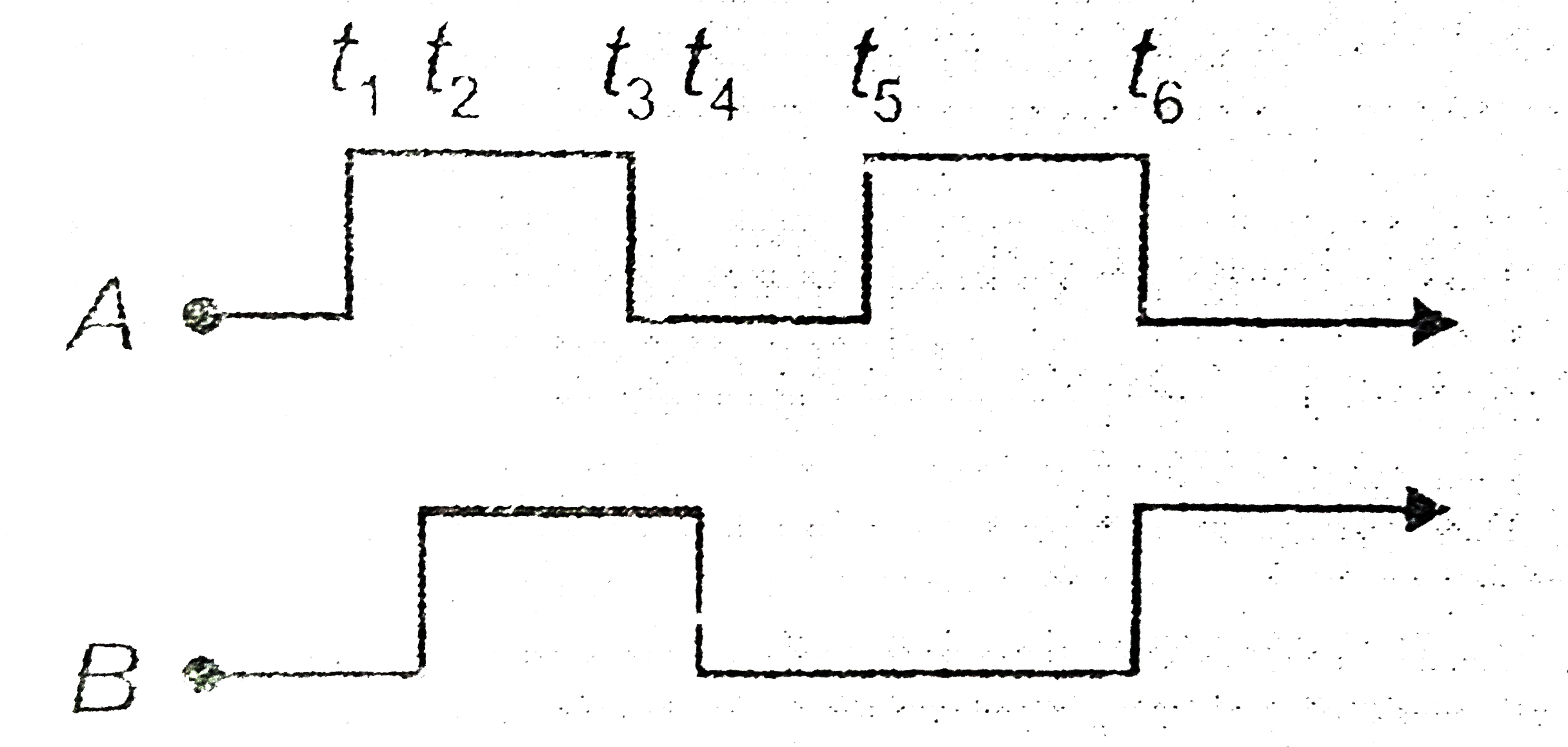
Sketch the output waveform obtained from AND gate for the following inputs A and B.
 View Solution
Sketch the output waveform obtained from AND gate for the following inputs A and B.
 View Solution
Write the output waveform of the OR gate for the inputs
View Solution(a) In the figure given below the input waveform is converted into the output waveform by a device 'X'. Name the device and draw its circuit diagram.

(b) Identify the logic gate represented by the circuit as shown and write its truth table.
 View Solution
Sketch the output waveform Y from a NAND gate having following inputs A and B
 View Solution
Sketch the output waveform Y from a NAND gate having following inputs A and B
 View Solution

