Transfer characteristics vs input volage for a base biased transistor in CE configuration for using transistor as a switch it is used
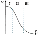
in region I
in region II
both in region I and III
in region II
EE=2.5eV=2.5×1.6×10−19J
hcλmax=4×10¹⁹J
=4.9695×10⁻⁷m=4969.5×10−10m
Hence diode can detect signal of wavelength less than calculated λmax
most appropriate signal is 400 A
Topper's Solved these Questions
- BOOK - MODERN PUBLICATIONCHAPTER - SEMICONDUCTOR ELECTRONICS METERIALS DEVICES AND SIMPLE CIRCUITS EXERCISE - COMPETION FILE (JEE(MAIN) & OTHER STATE BOARDS FOR ENGINEERING ENTRANCE )31videos
SEMICONDUCTOR ELECTRONICS METERIALS DEVICES AND SIMPLE CIRCUITS
- BOOK - MODERN PUBLICATIONCHAPTER - SEMICONDUCTOR ELECTRONICS METERIALS DEVICES AND SIMPLE CIRCUITS EXERCISE - COMPETION FILE( MULTIPLE CHOICE QUESTIONS )17videos
SEMICONDUCTOR ELECTRONICS METERIALS DEVICES AND SIMPLE CIRCUITS
- BOOK - MODERN PUBLICATIONCHAPTER - SEMICONDUCTOR ELECTRONICS METERIALS DEVICES AND SIMPLE CIRCUITS EXERCISE - REVISION EXERCISES (NUMERICAL PROBLEMS )15videos
SEMICONDUCTOR ELECTRONICS METERIALS DEVICES AND SIMPLE CIRCUITS
- BOOK - MODERN PUBLICATIONCHAPTER - RAY OPTICS AND OPTICAL INSTRUMENTSEXERCISE - CHAPTER PRACTICE TEST14videos
RAY OPTICS AND OPTICAL INSTRUMENTS
- BOOK - MODERN PUBLICATIONCHAPTER - WAVE OPTICALEXERCISE - CHAPTER PRACTICE TEST7videos
WAVE OPTICAL
Similar Questions
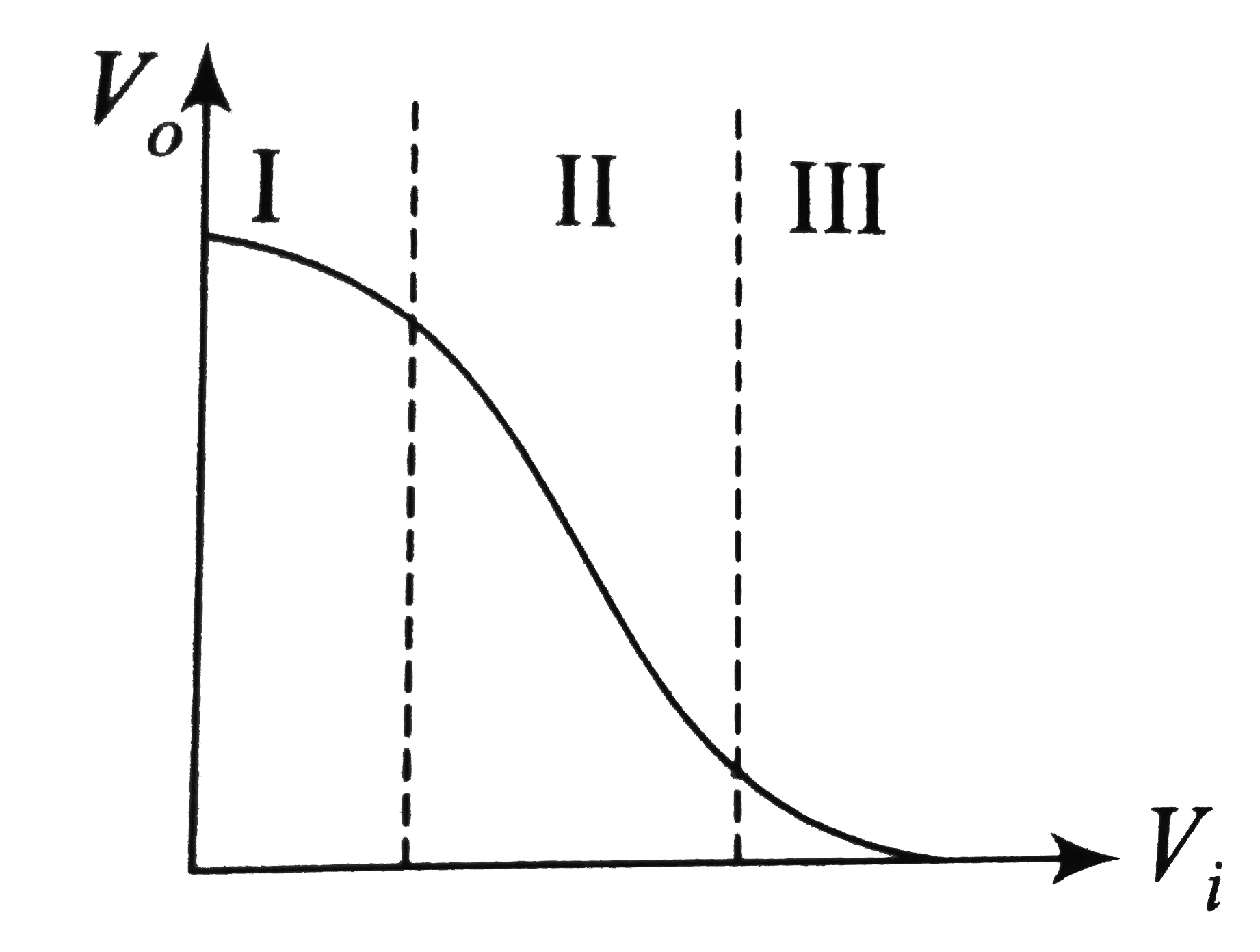
Transfer characterstics [output voltage (Vo) vs. input voltage (Vi)] for a base biased transistor in CE configuration is as shown in the figure. For using transfor as a which, it is used
 View Solution
Draw the transfer characteristic curve of a base biased transistor in CE configuration. Explain clearly how the active region of the Vo versus Vi curve in a transistor is used as an amplifier.
View Solution
Knowledge Check
- Question 1 - Select One
ट्रांजिस्टर के विभिन्न विन्यासो (configurations ) का वर्णन करे ।
AInput resistance is very large while output resistance is very smallBinput resistance is very small while output resistance is very highCboth input and output resistance are very smallDboth input and output resistances are very large - Question 2 - Select One
Transfer characterstics [output voltage (Vo) vs. input voltage (Vi)] for a base biased transistor in CE configuration is as shown in the figure. For using transfor as a which, it is used
 Ain region IBin region IIICboth in regios (I) and in (III)Din region II
 - Question 3 - Select One or More
Fig.shows that transfer characteristics of a base biased CE transistor. Which of the following statements are true?
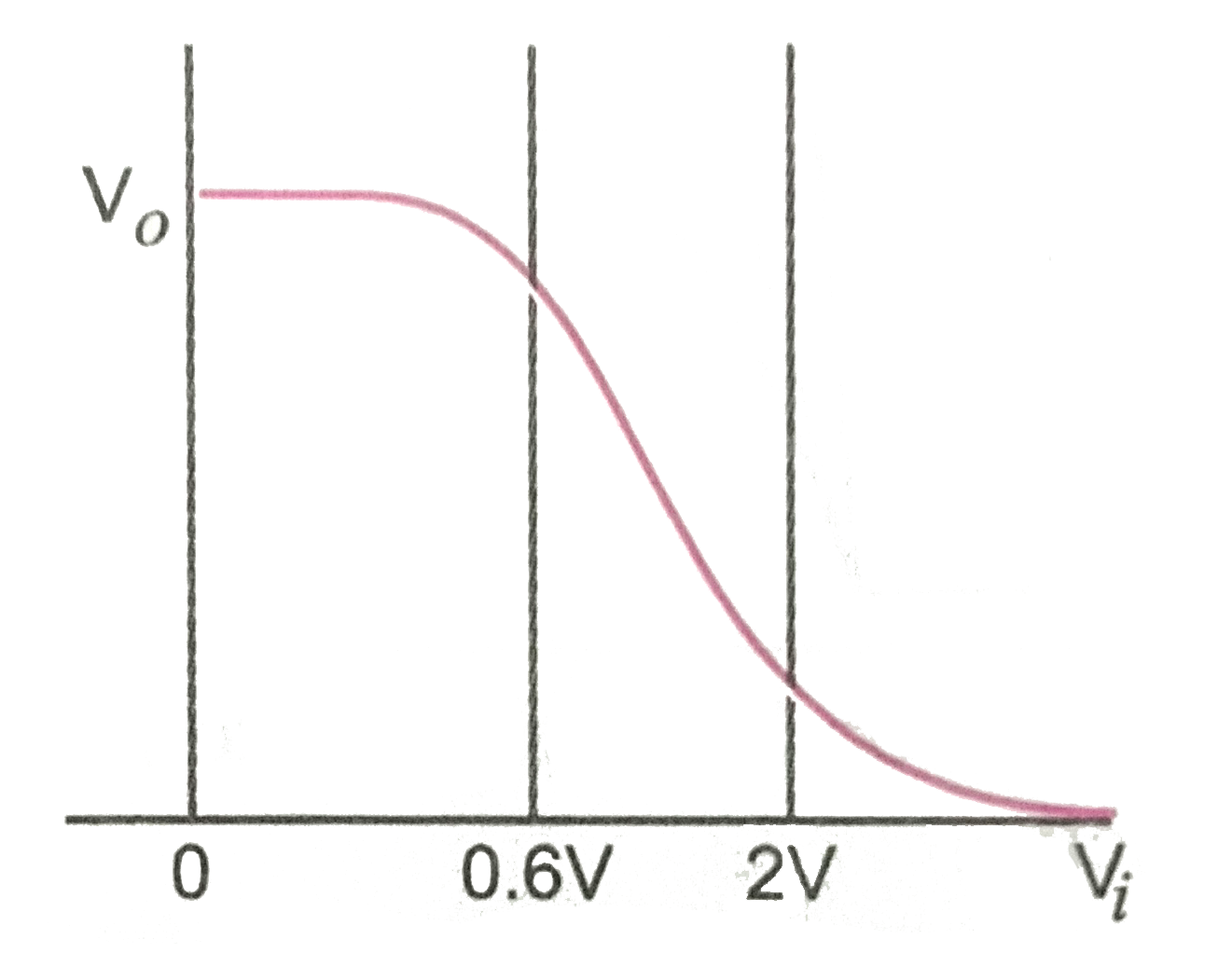 AAt Vi=0.4V, transistor is in active stateBAt Vi=IV, it can be used as an amplifierCAt Vi=0.5V, it can be used as a switch turned offDAt Vi=2.5V, can be used as a switch turned on
Explain, how a CE transistor acts as a switch.
View SolutionDraw the tramsfer characteristic curve of a base biased transistor in CE configuration. Explain clearly how the active region of the Vo versus Vi curve in a transistor is used as an amplifier.
View SolutionDraw the tramsfer characteristic curve of a base biased transistor in CE configuration. Explain clearly how the active region of the Vo versus Vi curve in a transistor is used as an amplifier.
View SolutionIn a transistor in CE configuration, the ratio of power gain to voltage gain is
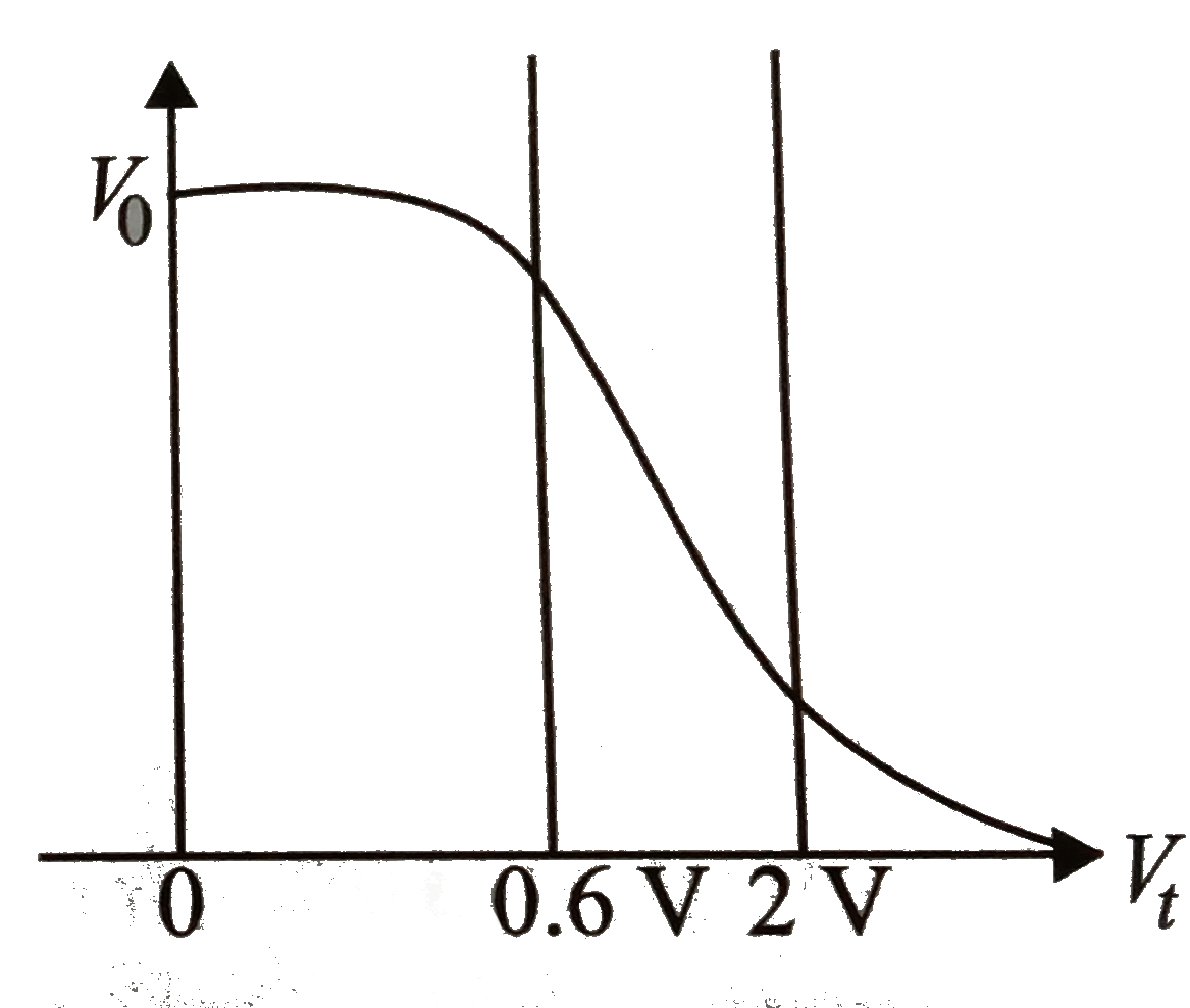
View SolutionThe transfer characteristics of a base biased common emitter transistor is shown in the figure. Which of the following statements are true?
 View Solution
