Draw the tramsfer characteristic curve of a base biased transistor in CE configuration. Explain clearly how the active region of the curve in a transistor is used as an amplifier.
(a) 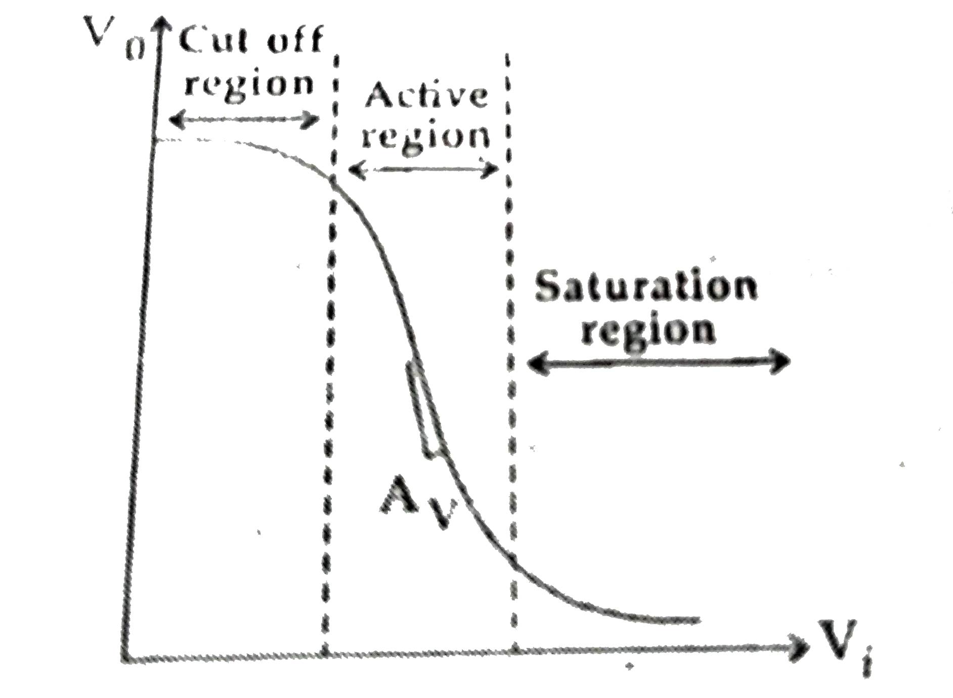
In the active region, a (samll) increase of Vi results in a (large, almost linear) increase in . This results in an increase in the voltage drop across .
(b) When becomes greater than 0.6 V, the transistor is an active state with some current. in the output path. The transistor is operated as a switch. As long as is low and unable to forward-bias the transistor, is high enough to derive the transistor into saturation, the is low, very near to zero.
When the transistor is not conducting, it is said to be switched off and when it is driven into saturation,
Topper's Solved these Questions
- BOOK - XII BOARD PREVIOUS YEAR PAPER ENGLISHCHAPTER - XII BOARDSEXERCISE - SET-II, DELHI BOARD4videos
XII BOARDS
- BOOK - XII BOARD PREVIOUS YEAR PAPER ENGLISHCHAPTER - XII BOARDSEXERCISE - SET-III, DELHI BOARD4videos
XII BOARDS
- BOOK - XII BOARD PREVIOUS YEAR PAPER ENGLISHCHAPTER - XII BOARDSEXERCISE - SET -III4videos
XII BOARDS
- BOOK - XII BOARD PREVIOUS YEAR PAPER ENGLISHCHAPTER - SAMPLE PAPER 2019EXERCISE - SECTION D6videos
SAMPLE PAPER 2019
Similar Questions
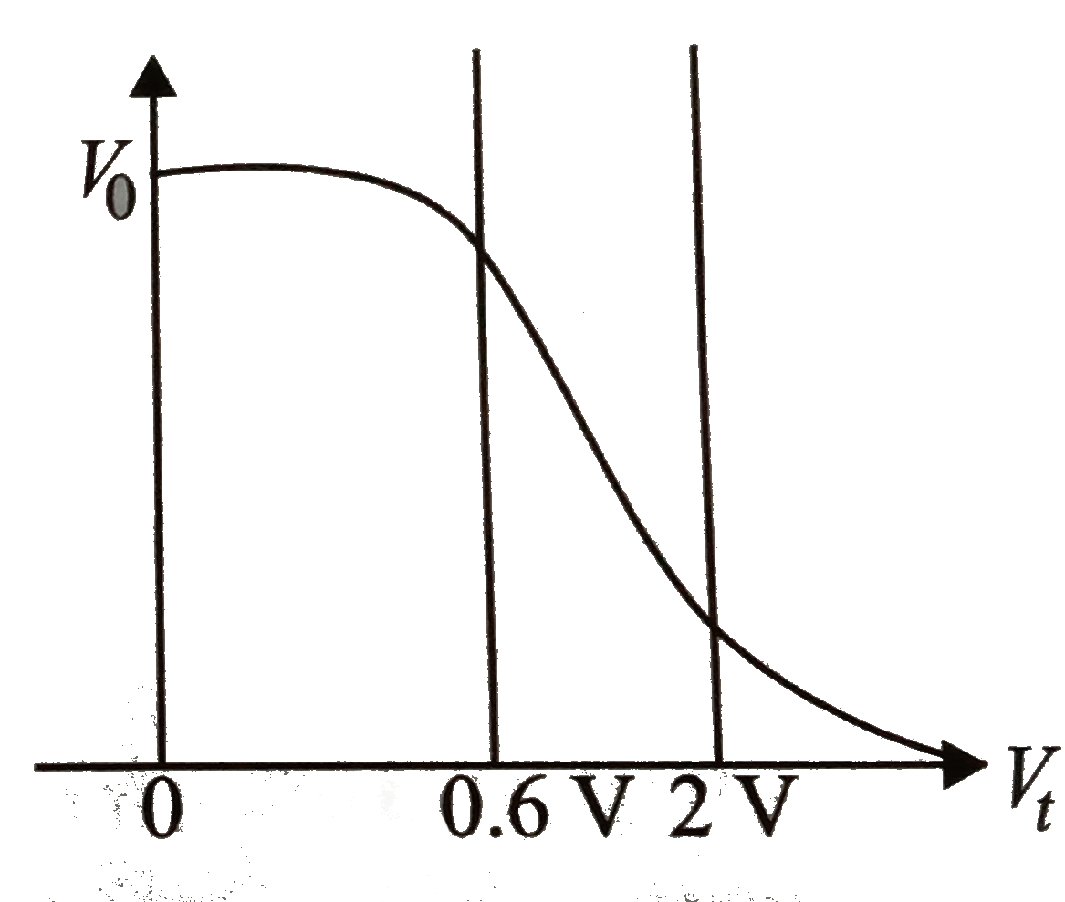
The transfer characteristics of a base biased common emitter transistor is shown in the figure. Which of the following statements are true?
 View Solution
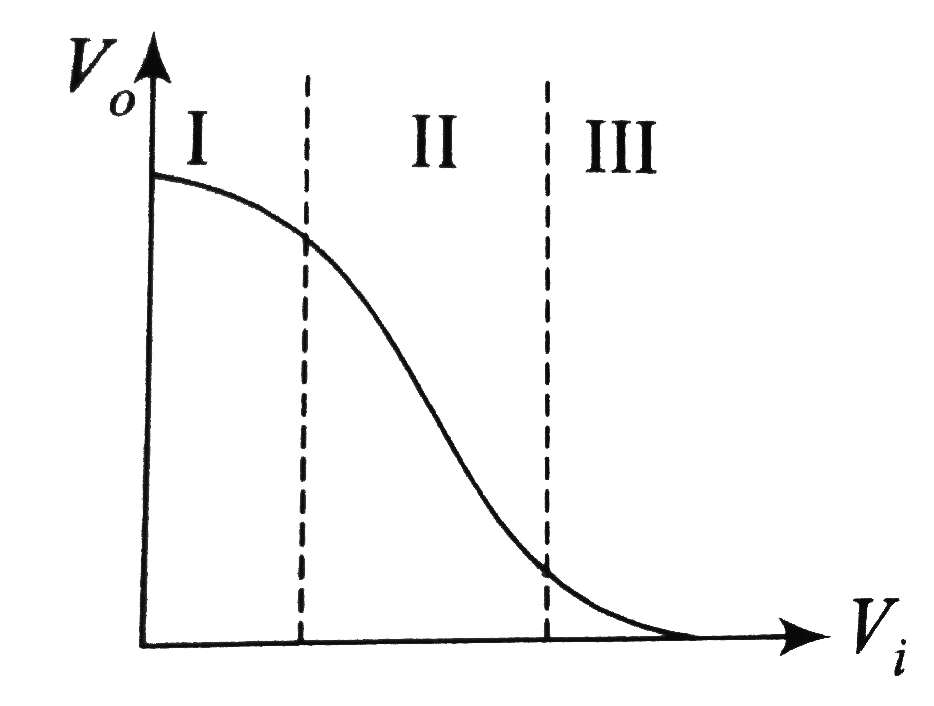
Transfer characterstics [output voltage (Vo) vs. input voltage (Vi)] for a base biased transistor in CE configuration is as shown in the figure. For using transfor as a which, it is used
 View Solution
Knowledge Check
- Question 1 - Select One
The transfer characteristics of a base biased transistor has the operation regions, namely, cutoff, active region and saturation region. For using the transistor as an amplifier it has to operate in the
Aactive regionBcutoff regionCsaturation regionDcutoff and saturation - Question 2 - Select One
Fig.shows that transfer characteristics of a base biased CE transistor. Which of the following statements are true?
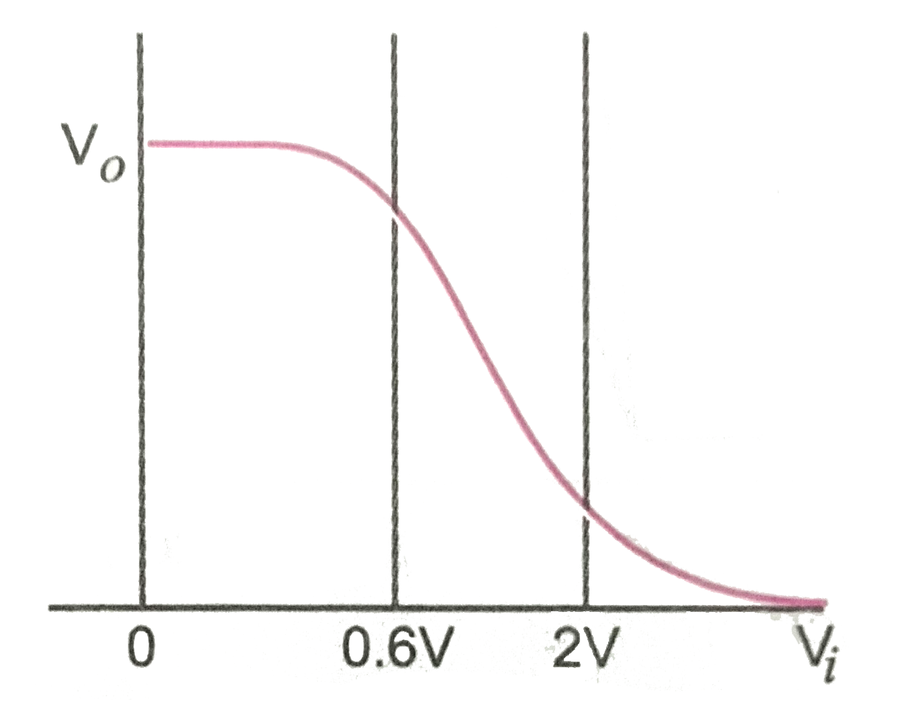 AAt Vi=1V, it can be used as an amplifierBAt Vi=0.5V, it can be used as a switch turned offCAt Vi=2.5V, it can be used as a switch turned onDAll of these
Draw a labelled circuit diagram of n - p - n germanium transistor in common emitter configuration. Explain briefly, how this transistor is used as a voltage amplifier.
View SolutionDraw typical output characteristics of an n-p-n transistor in CE configuration. Show how these characteristics can be used to determine output resistance.
View SolutionDraw the labelled circuit diagram of a common-emitter transistor amplifier : Explain clearly how the input and output signals are in opposite phase.
View SolutionDraw the diagram of the circuit arangement used for studying the 'input' and the 'output' characteristics of an n-p-n transistor inits CE configuration. Briefly explain how these two types of characteristics are obtained and draw these characteristics.
(b) 'Define' the terms (i) Input resistance, (ii) Output resistance , (iii) Current amplification factor, for a given transistor.View Solution(a) Draw the circuit arrangement for studying the input and output characteristics of an n-p-n transistor in CE configuration . With the help of these characteristics define (i) input resistance , (ii) current amplification factor .
(b) Describe briefly with the help of a circuit diagram how an n-p-n transistor is used to produce self-sustained oscillations .View Solution(i) Figure shows the input waveform which is converted by a device .X. into an output wavefrom. Mane the device and explain its working using the proper circuit.
(ii) Draw the forward bias and reverse blas circuit for the basic component of the device and draw the characterstics.
Explain clearly which region of the curve is used in an amplifier.View Solution

