Complete Solutions to Level-II (H.W) of chapter SEMI CONDUCTOR DEVICES of Class 12 book with complete answers and questions
| Class 12 | PHYSICS |
| Chapter | SEMI CONDUCTOR DEVICES |
| NARAYANA | Level-II (H.W) |
| Number Of Questions | 36 |
| Academic Year | 2023-24 |
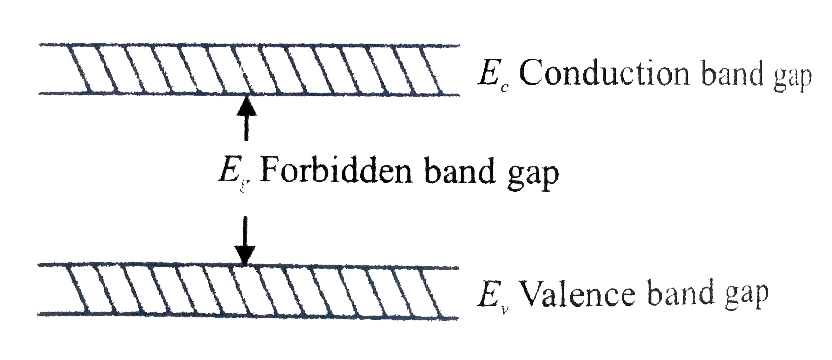
If the lattice constant of this semiconductor is decreased, then which of the following is correct ?
 .03:05View Solution
A `Ge` specimen is dopped with `Al`. The concentration of acceptor atoms is `~10^(21) at oms//m^(3)`. Given that the intrinsic concentration of electron hole pairs is `~10^(19)//m^(3)`, the concentration of electron in the speciman is
02:45View SolutionThe following data are for intrinsic germanium at `300 K. n_(i) = 2.4 xx 10^(19)//m^(3), mu_(e) = 0.39 m^(2)//Vs, mu_(h) = 0.19 m^(2)//Vs`. Calculate the coductivity of intrinsic germanium.
02:21View SolutionThe diagram correctly represents the direction of flow of charge carriers in the forward bias of `p-n` junction is.
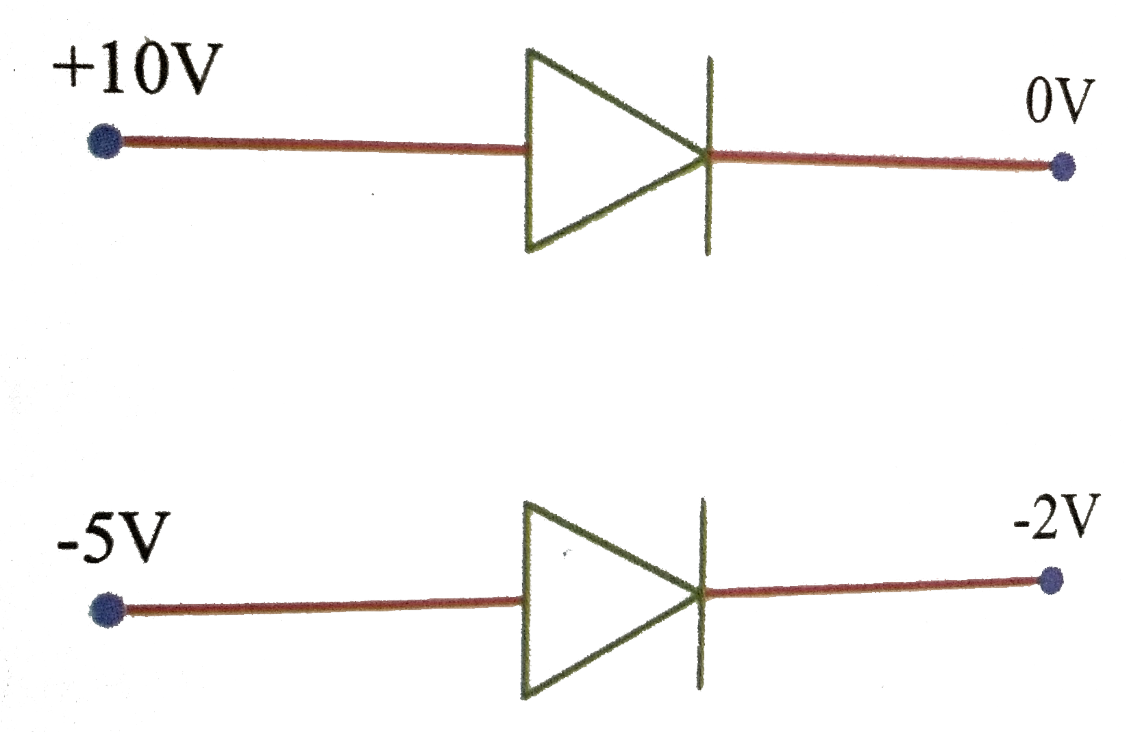
03:00View SolutionIn the figure shown below
 .02:12View Solution
A `P-N` junction diode can withstand currents up to `10 mA`. Under forward bias, The diode has a potential drop of `0.5 V` across it which is assumed to be independent of current. The maximum voltage of the battery used to forward bias the diode when a resistance of `200 Omega` is connected in series with it is
02:34View SolutionA cell of emf. `4.5 V` is connected to a junction diode whose barrier potential is `0.7 V`. If the external resistance in the circuit is `190 Omega`. The current in the circuit is
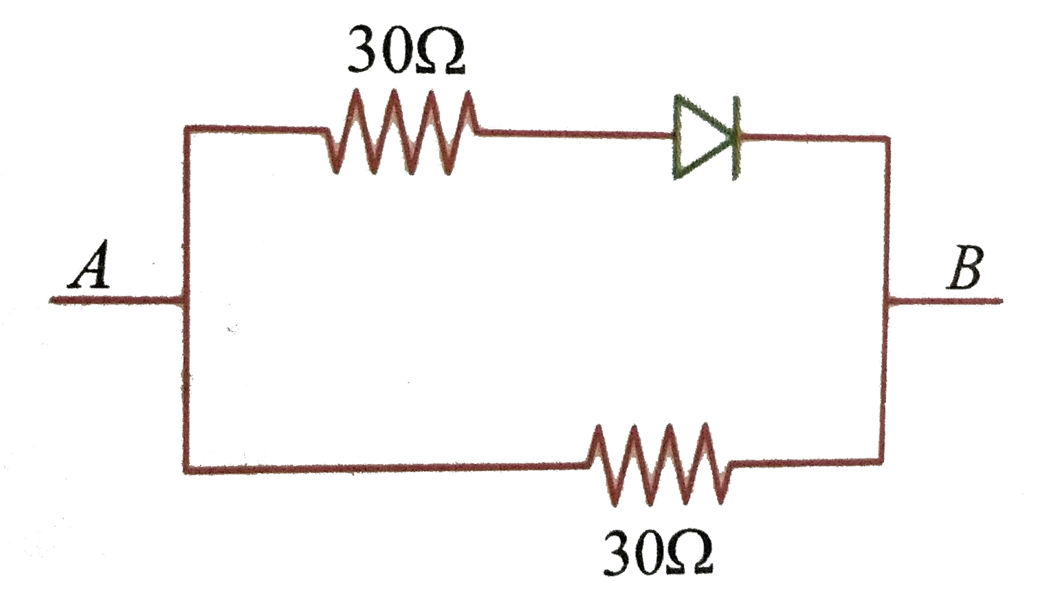
02:30View Solution`V_(A)` and `V_(B)` denote potential of `A` and `B`, then the equivalent resistance between `A` and `B` in the adjoining circuit is (ideal diode).
 .03:13View Solution
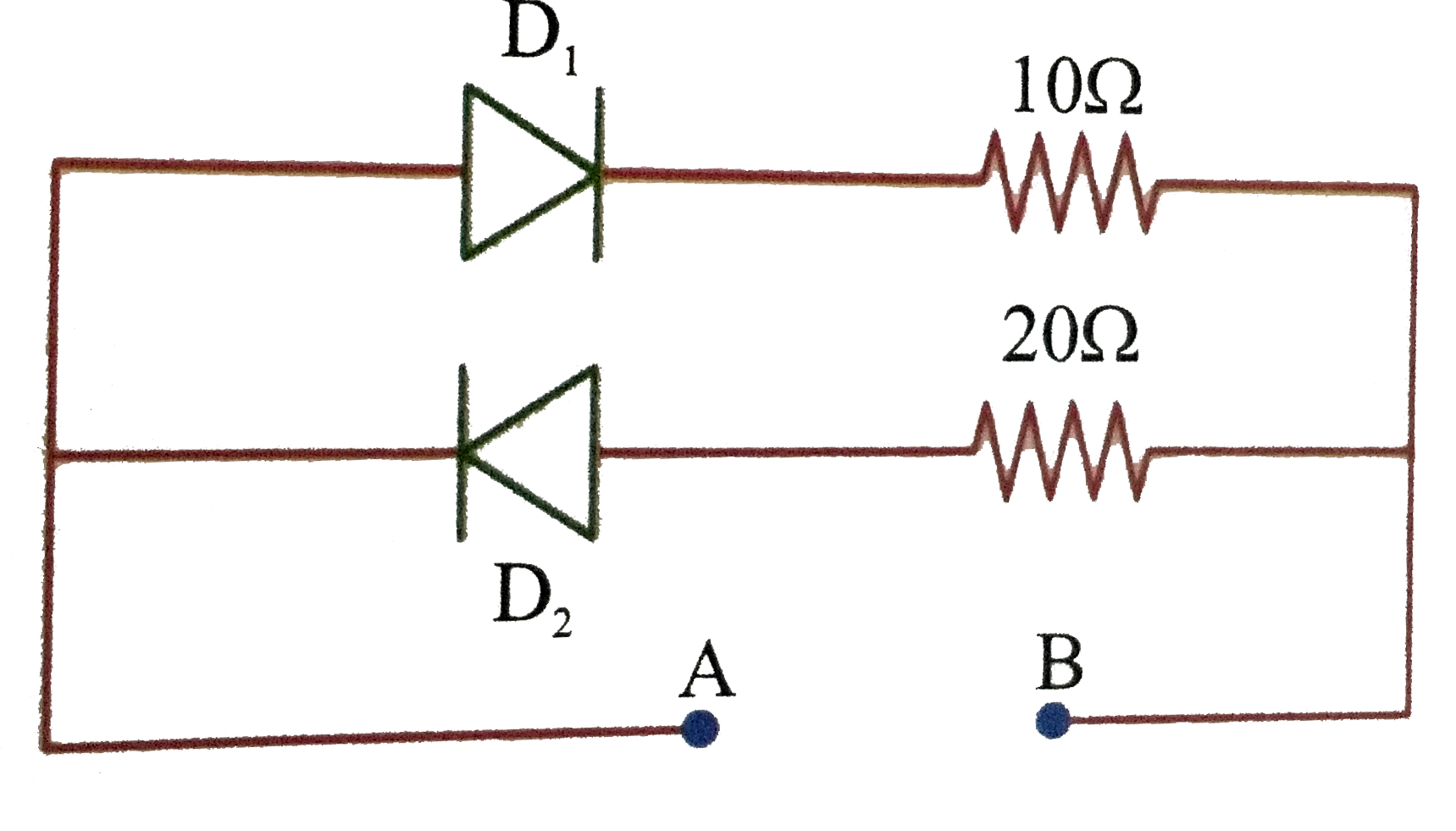
Two ideal junction diodes `D_(1),D_(2)` are connected as shown in the figure. A `3V` battery is connected between `A` and `B`. The current supplied by the battery if its positive terminal is connected to `A` is
 .02:08View Solution
Find the effective resistance between `A` and `B`
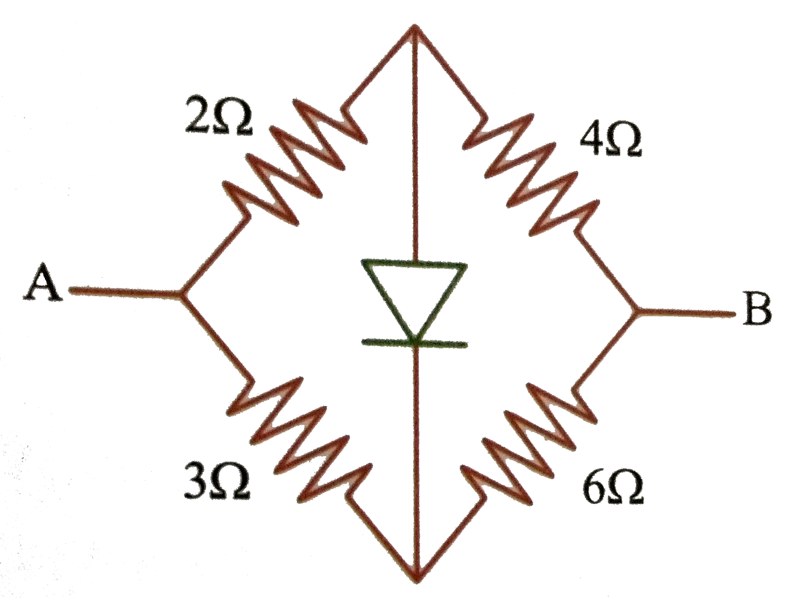 .03:30View Solution
The peak voltage in the output of a half-wave diode rectifier fed with a sinusiodal signal without filter is `10 V`. The `dc` component of the output voltage is
01:24View SolutionIn the figure shown the potential drop across the series resistor is
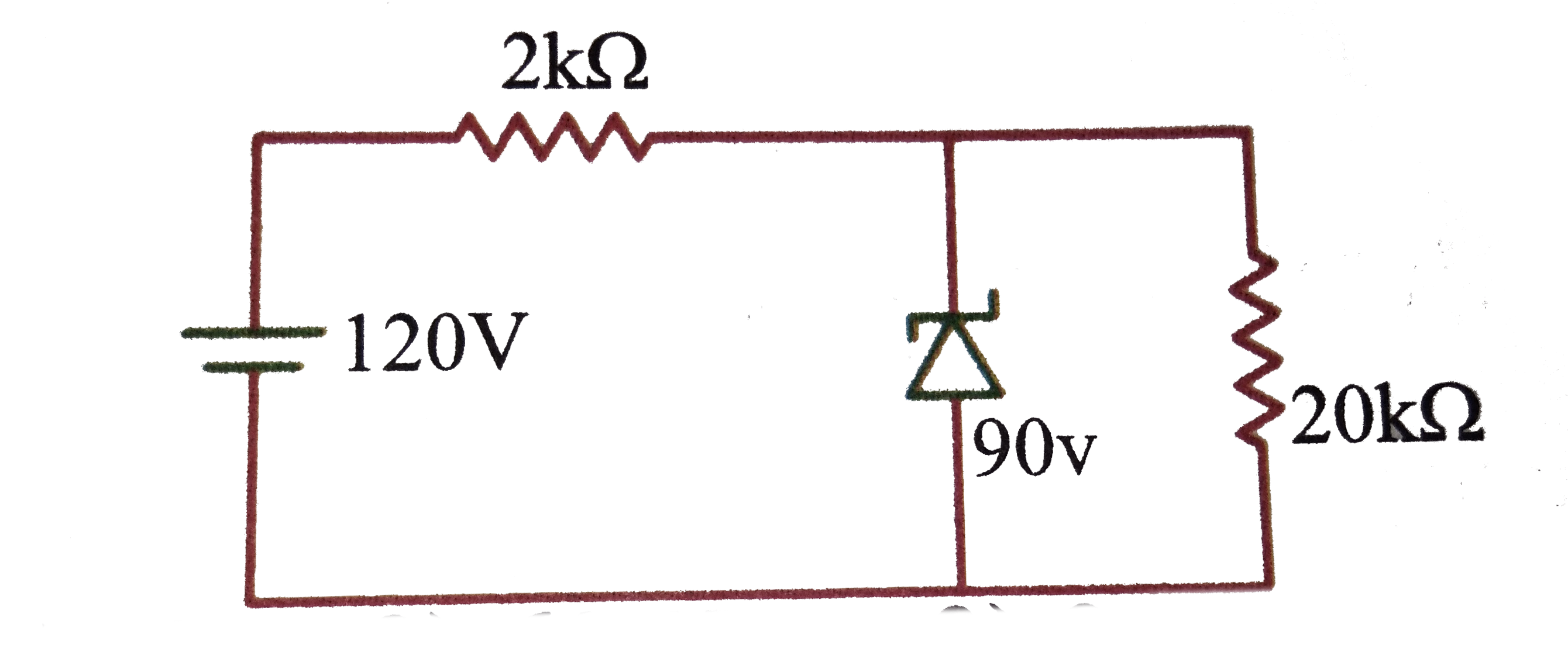 01:59View Solution
A 220 V AC supply is connected between points A and B . What will be the potential difference V across the capacitor ?
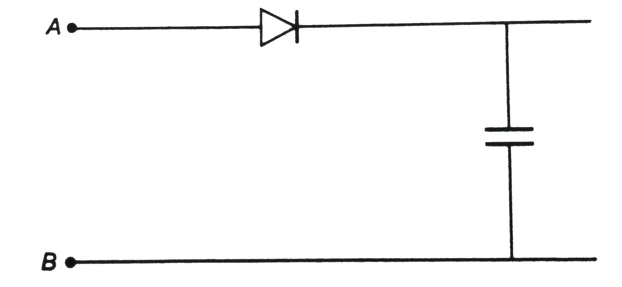 01:35View Solution
In the circuit shown(Fig.) if the diode forward voltage drop is `0.3 V`, the voltage difference between `A` and `B` is :
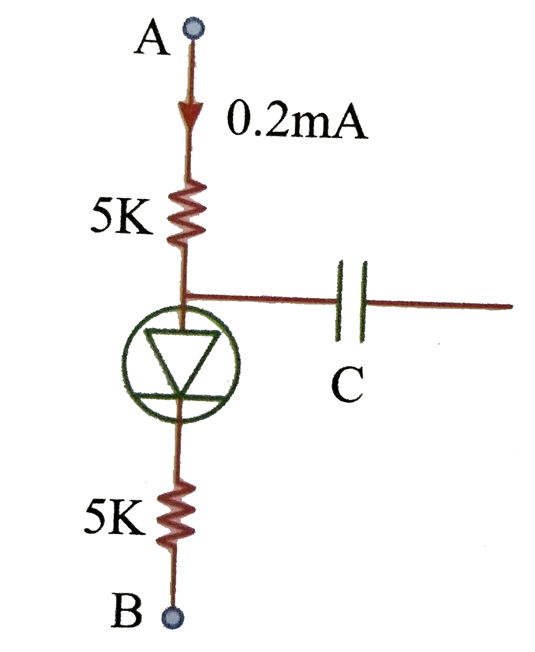 .02:45View Solution
In an n-p-n transistor `10^(10)` electrons enter the emitter in `10^(-6)`s. If 2% of the electrons are lost in the base, find the current transfer ratio and the current amplification factor.
02:52View SolutionIn a common base mode of transistor, collector current is `5.488 mA` for an emitter current of `5.60mA`. The value of the base current amplification factor `(beta)` will be :
01:48View SolutionCurrent amplification factor of a common base configuration is `0.88`. Find the value of base current when the emitter current is `1 m A`.
01:42View SolutionFor a transistor `beta = 40` and `I_(B) = 25 muA`. Find the value of `I_(E)`.
01:59View SolutionIn a transistor if `(I_(C))/(I_(E))=alpha` and `(I_(C))/(I_(B))=beta`,If `alpha` varies between `(20)/(21) and (100)/(101)`, then the value of `beta` lied between.
03:15View SolutionFor a transistor `x=(1)/(alpha)&y=(1)/(beta)` where `alpha & beta` are current gains in common base and common emitter configuration. Then
01:57View SolutionA voltage amplifier operated from a 12 volt battery has a collector load `6 k Omega`. Calculate the maximum collector current in the circuit.
01:27View SolutionA `CE` amplifier is designed with a transistor having `alpha =0.99`. Input impedance is `1 k Omega` and load is `10 k Omega`. Voltage gain will be :
02:01View SolutionIn a common emitter amplifier the load resistance of the output circuit is `792` times the resistance of the input circuit. If `alpha = 0.99`. The voltage gain is.
04:16View SolutionIn a transistor amplifier `beta = 62, R_(L) = 5000 Omega` and internal resistance of the transistor is `500 Omega`. Its power amplification will be.
01:35View SolutionThe tuned collector oscillator circuit used in the local oscillator of a ratio receiver makes use of a tuned circuit with `L = 60 mu H` and `C = 400 pE`. Calculate the frequency of oscillations.
02:10View SolutionWhen we add binary number `111` and `111` we get the binary number :
01:30View SolutionIf `A =B=C=1` and `X= overline(ABC)+B overline(BC) + C overline(AB)`, then `X=`
02:44View SolutionThe input of `A` and `B`for the Boolean expression `(overline(A+B)).(overline(A.B))=1` is.
01:54View SolutionWrite the truth table for the circuit shown in figure given below. Name the gate that the circuit resembles.
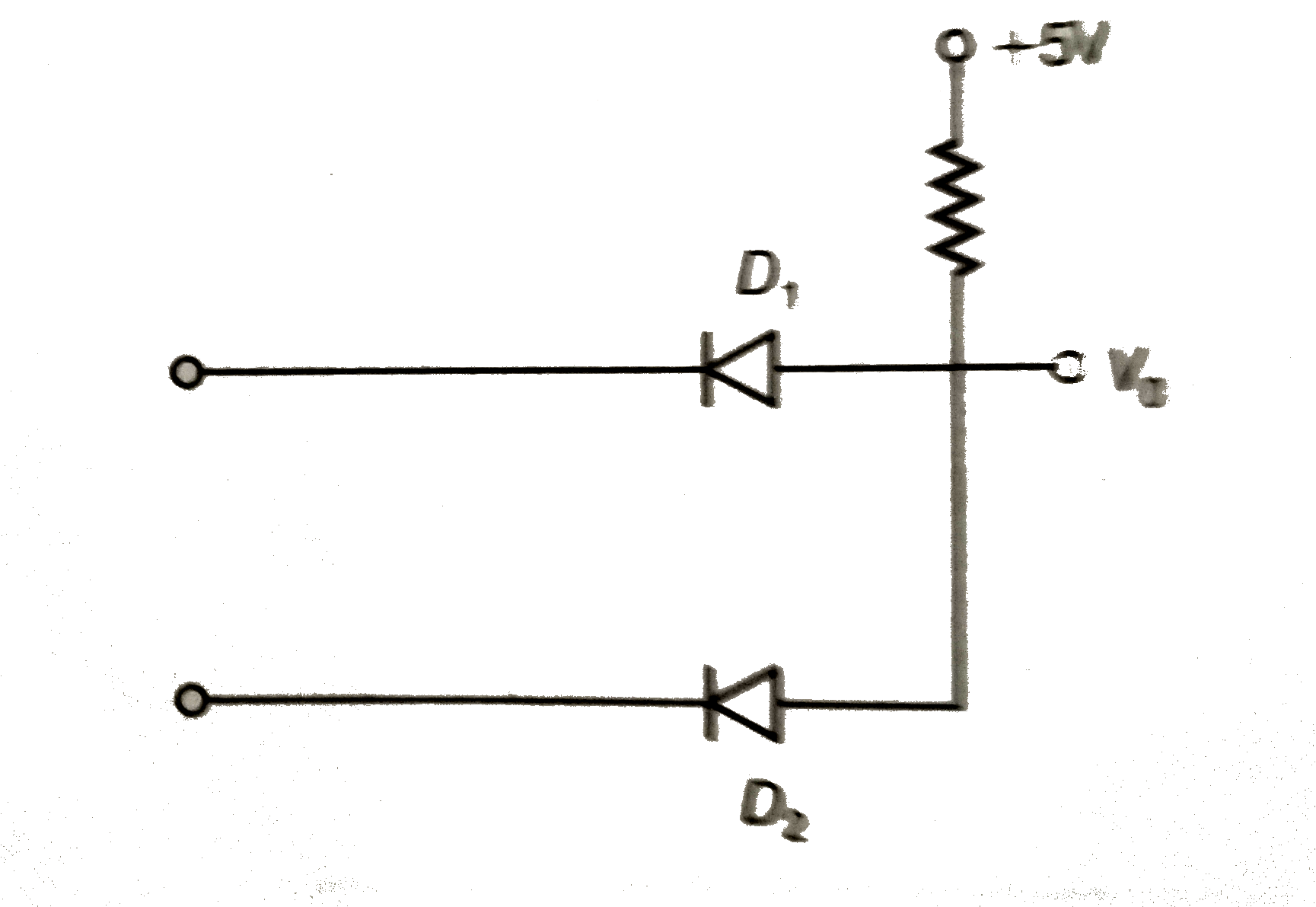 04:05View Solution
Consider a two-input `AND` gate of figure below. Out of the four entries for the Truth Table given here, the correct ones are.
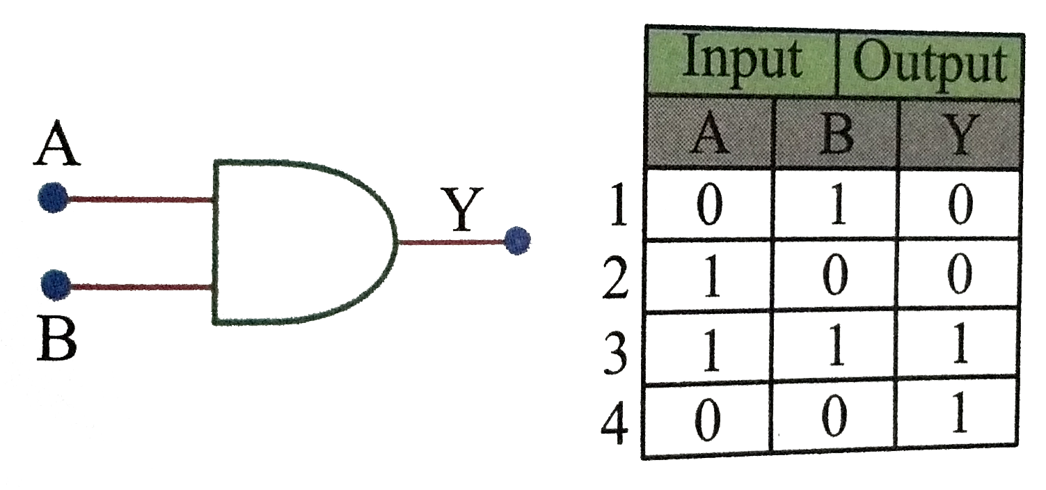 .01:39View Solution
A Truth table is given below. The below. The logic gate having following truth table is.
`{:(A,B,Y),(0,0,1),(1,0,0),(0,1,0),(1,1,0):}`.01:57View SolutionFor a logic `0101` the waveform is.
02:08View SolutionFor the given combination of gates, if the logic states of inputs `A,B,C` are as follows `A=B=C=-0` and `A=B=1,C=0` then the logic states of output `D` are
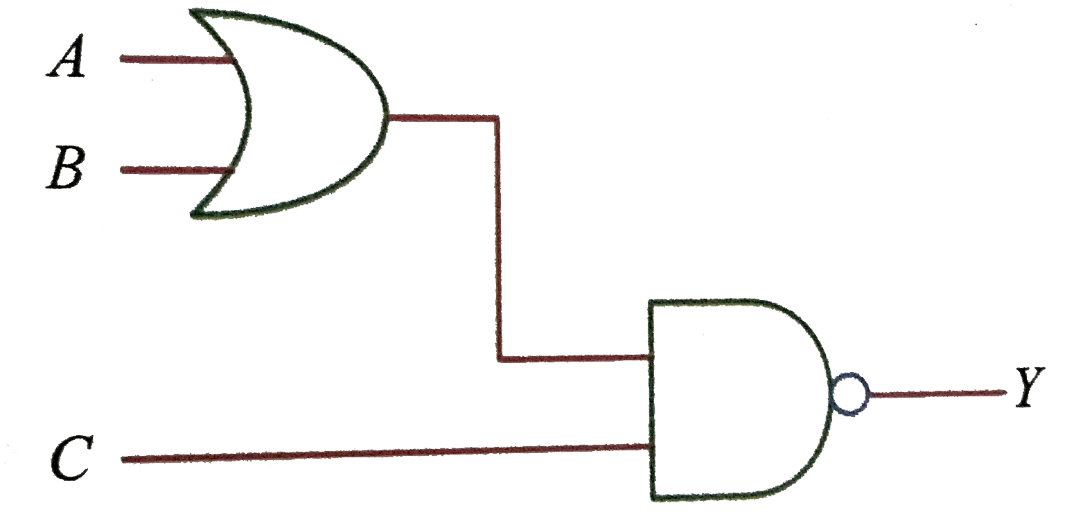 02:26View Solution
Identify the gate represented by the block diagram as shown in fig.
 01:49View Solution
The Boolean expression for the gate circuit shown below is
 01:45View Solution
The output `Y` of the gate circuit shown in the figure below is
 01:28View Solution
Level-II (H.W) questions and complete solutions for chapter SEMI CONDUCTOR DEVICES of NARAYANA PHYSICS (HINGLISH) of Class 12
