Complete Solutions to Solved Example of chapter SEMI CONDUCTOR DEVICES of Class 12 book with complete answers and questions
| Class 12 | PHYSICS |
| Chapter | SEMI CONDUCTOR DEVICES |
| NARAYANA | Solved Example |
| Number Of Questions | 32 |
| Academic Year | 2023-24 |
The number of silicon atoms per `m^(3) is 5xx10^(28)`. This is doped simultaneously with `5xx10^(22)` atoms per `m^(3)` of Arsenic and `5xx10^(20) per m^(3)` atoms of indium. Calculate the number of electrons and holes. Given that `n_(i)=1.5xx10^(16)m^(-3)`. Is the material n-type or p-type?
03:29View SolutionA semiconductor has an electron concentration of `0.45 xx 10^(12) m^(-3)` and a hole concentration of `5.0 xx 10^(20) m^(-3)`. Calculate its conductivity. Given electron mobility `= 0.135 m^(2) V^(-1) s^(-1)`, hole mobility `= 0.048 m^(2) V^(-1) s^(-1)`,
02:50View SolutionA `N`-type silicon sample of width `4xx10^(-3)m`, thickness and length `6xx10^(-2)m` carriers a current of `4.8mA`, when the voltage is applied across the length of the sample. The free electron density is `10^(22)m^(-3)`
05:18View SolutionThe energy gap of pure `Si` is `1.1 eV` The mobilities of electrons and holes are respectively `0.135 m^(2) V^(-1) s^(-1)` and `0.048 m^(2) V^(-1) s^(-1)` and can be taken as independent of temperature. The intrinsic carrier concentration is given by `n_(i) = n_(0) e^(-Eg//2kT)`.
Where `n_(0)` is a constant, `E_(g)` The gap width and `k` The Boltmann's constant whose vaue is `1.38 xx 10^(-23) JK^(-1)` The ratio of the electrical conductivities of `Si` at `600 K` and `300 K` is.05:39View SolutionIn a `p-n` junction diode, the currect `I` can expressed as `I=I_(0) exp((eV)/(2k_(B)T)-1)` where `I_(0)` is called the reverse saturation current, `V` is the voltage across the diode and is positive for forward bias and negative for reverse bias, and `I` is the current through the diode, `K_(B)` is the Boltzmann constant `(8.6 xx 10^(-5) eV//K)` and `T` is the absolute temperature. If for a given diode `I_(o) = 5 xx 10^(-12) A` and `T = 300 K`, then
(a) What will be the forward current at a formward voltage of `0.6V` ?
(b) What will be the increase in the current if the voltage across the diode is increased to `0.7 V` ?
( c) What is the dynamic resistance ?
(d) What will be current if reverse bias voltage changes from `1 V` to `2 V` ?05:54View SolutionThe energy of a photon of sodium light `(lambda=589 nm)`equal the band gap of a semiconducting material.(a)Find the minimum energy E requried to create a hole-electron pair.(b)Find the value of `E//kT`at a temperature of 300K.
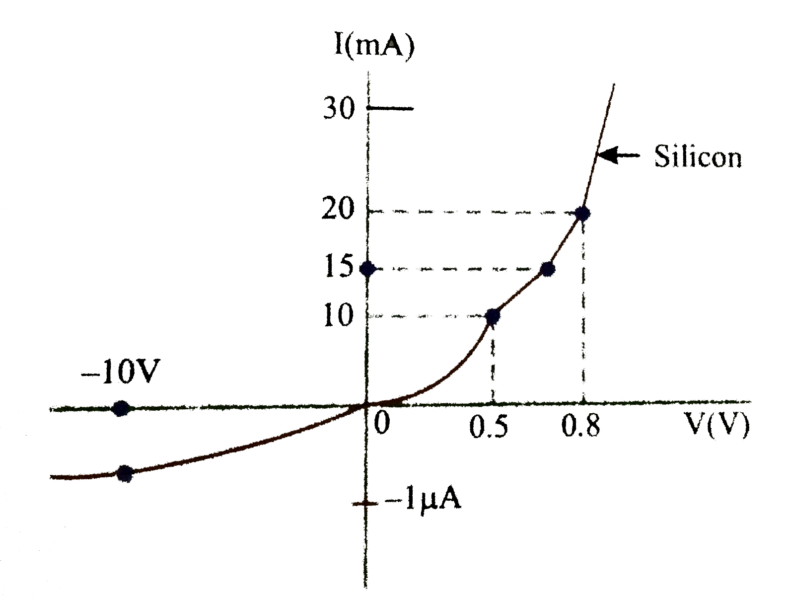
03:14View SolutionThe `V-I` characteristic of a silicon diode is shown in the Fig. Calculate the resistance of the diode at
(a) `I_(D) = 15 mA` and
(b) `V_(D) = -10 V`.
 .03:51View Solution
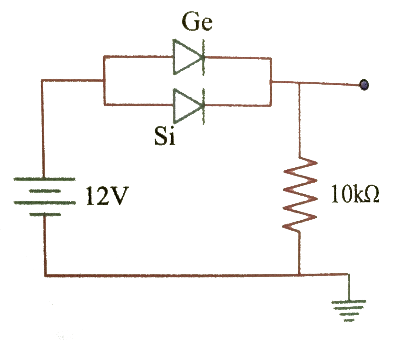
Two junction diodes, one of germanium `(Ge)` and other of silicon `(Si)` are connected as shown in fig to a battery of `12 V` and a load resistance `10 kOmega`. The germanium diode conducts at `0.3 V` and silicon diode at `0.7 V`. When current flows in the circuit, the potential of terminal `Y` will be
 .04:03View Solution
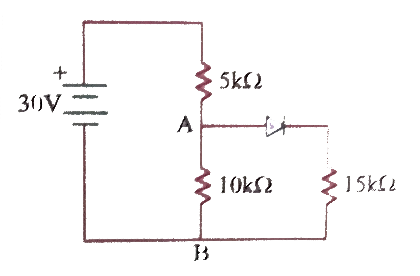
Find the maximum voltage across `AB` in the circuit shown in Fig. Assume that diode is ideal.
 .04:46View Solution
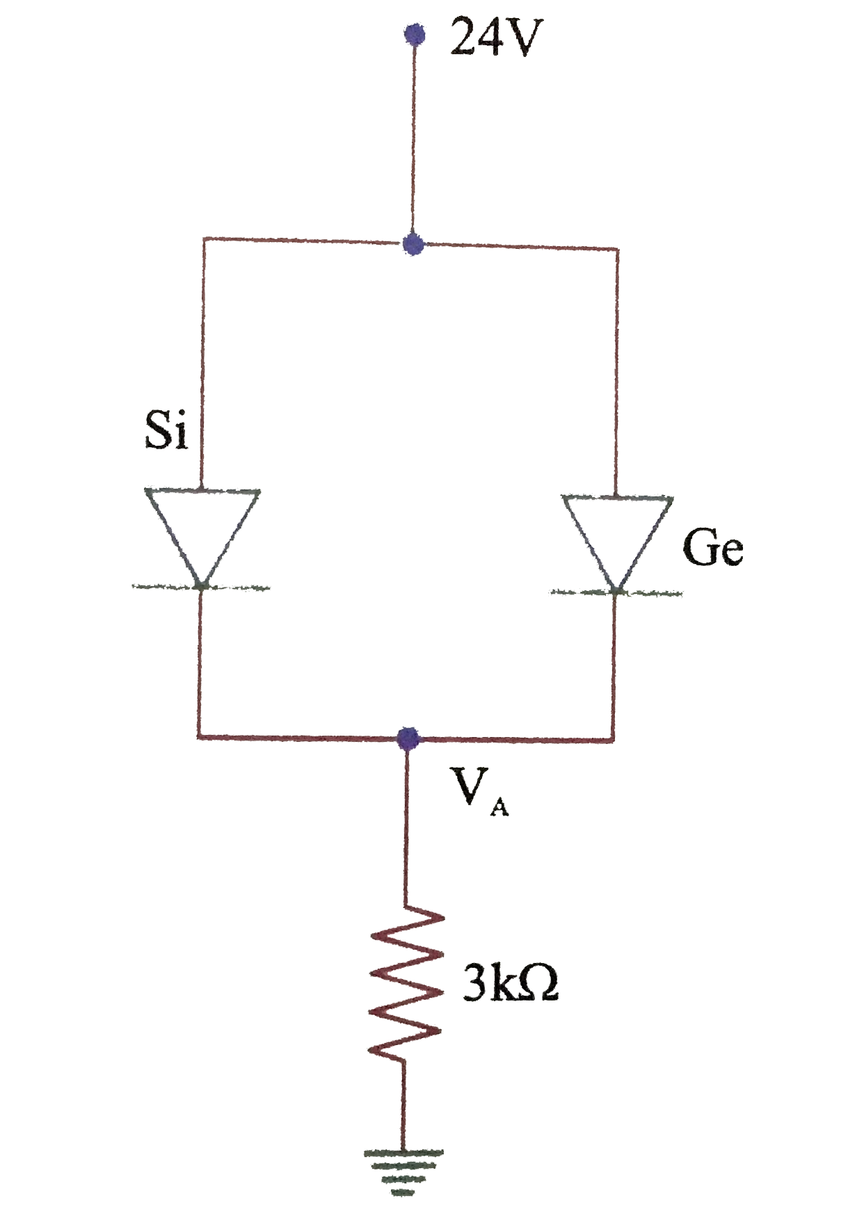
Find the voltage `V_(A)` in the curcuit shown in figure. The potential barrier for `Ge` is `0.3 V` and for `Si` is `0.7 V`
 .02:55View Solution
Considering the circuit and data given in the diagram, calculate the currents flowing in the diodes `D_(1)` and `D_(2)` Forward resistance of `D_(1)` and `D_(2)` is `20 Omega`.
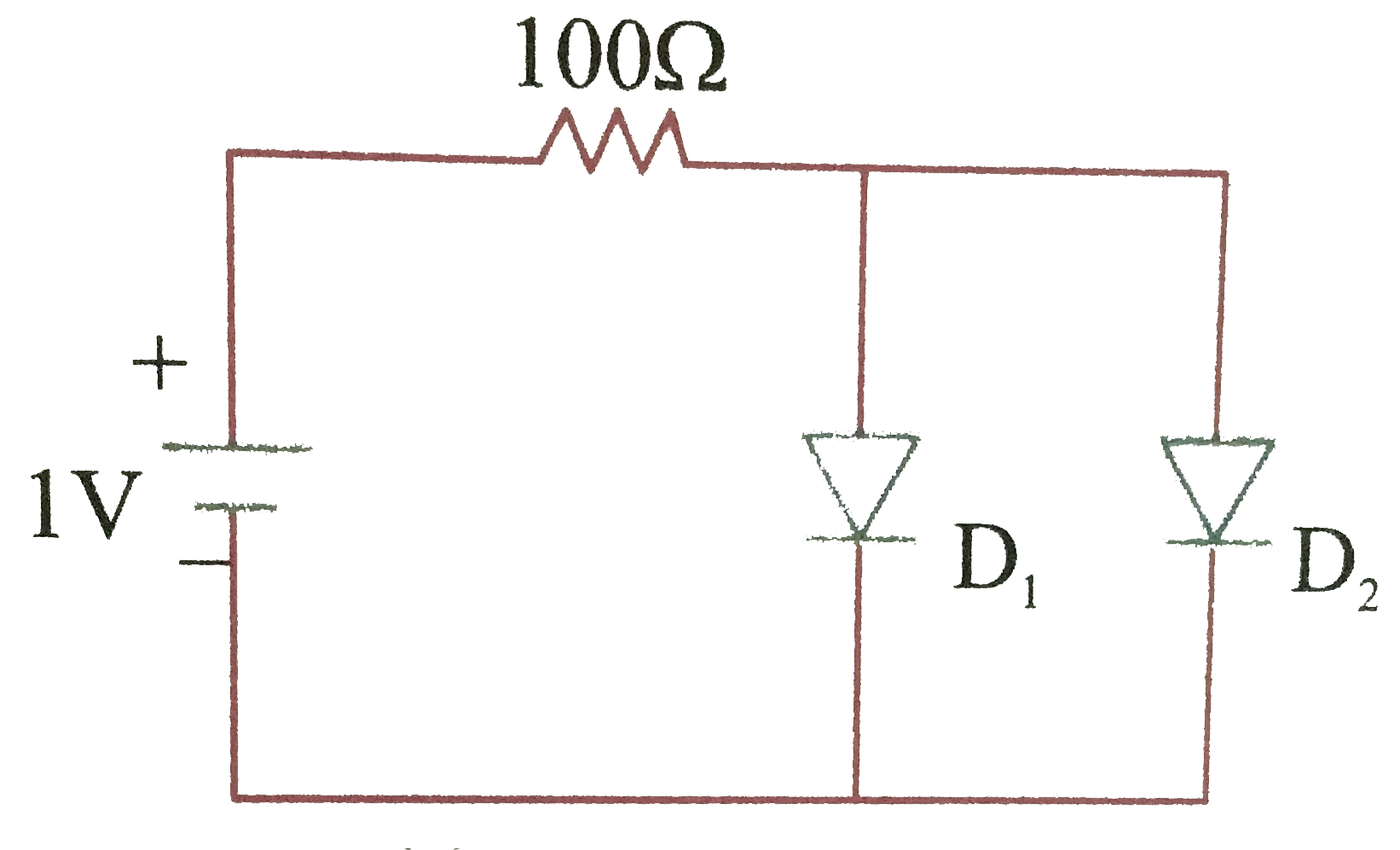 .04:31View Solution
In the circuit shown. The potential drop across each capacitor is (assuming the two diodes are ideal).
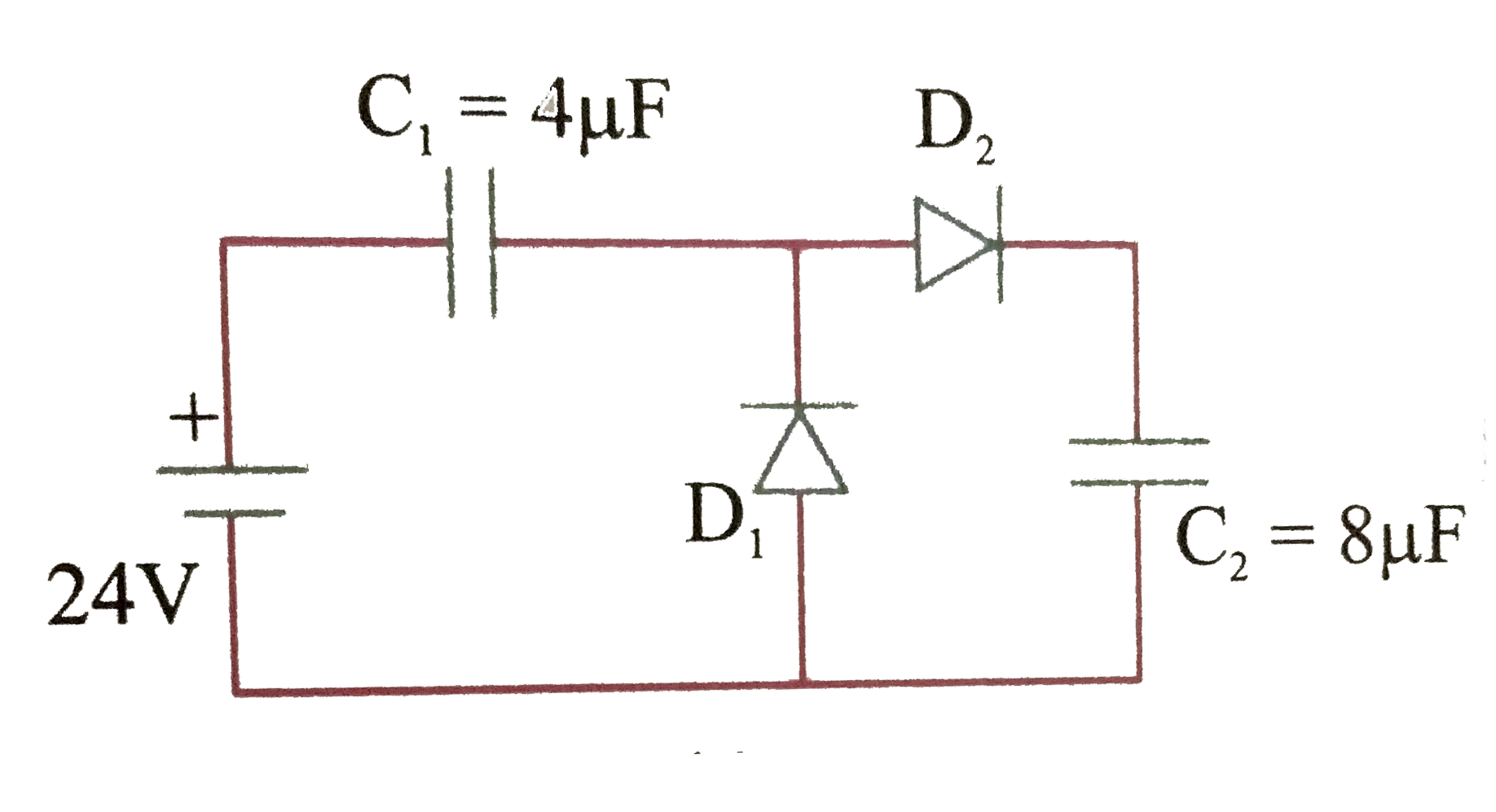 .04:06View Solution
A potential barrier of 0.50V exists across a p-n junction.(a) If the depletion region is `5.0xx10^(-7)`m wide,what is the intensity of the electric field in this region?(b) An electron with speed`5.0xx10^(5)m s^(-1)`approaches the p-n junction form the n-side.With what speed will it enter the p-side?
09:55View SolutionA `p-n` diode is used in a half wave rectifier with a load resistance of `1000 Omega`. If the forward resistance `(r_(f))` of diode is `10 Omega`, calculate the efficiency of this half wave rectifier.
01:51View SolutionA full wave rectifier uses two diodes with a load resistance of `100 Omega`. Each diode is having negligible forward resistance. Find the efficiency of this wave rectifier.
01:34View SolutionIf a `p-n` junction diode, a square input signal of `10 V` is applied as shown.
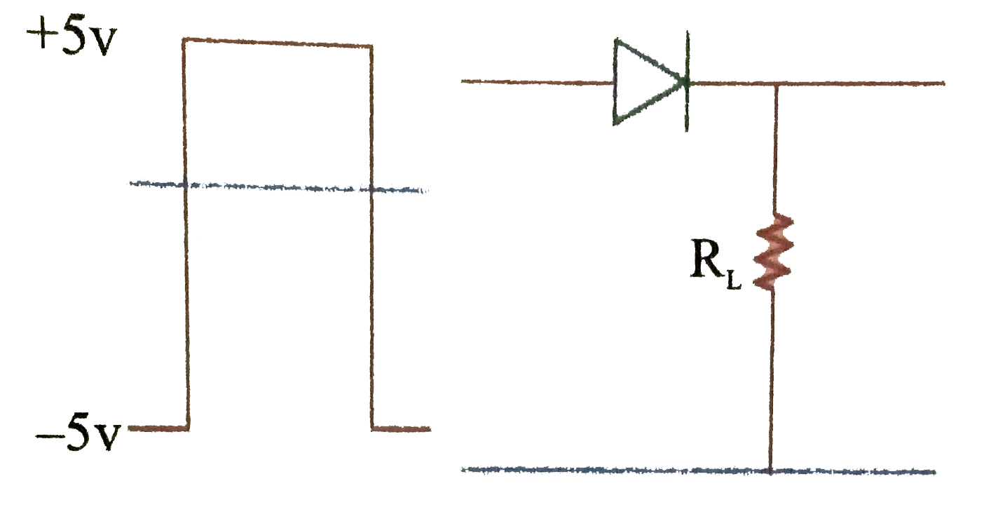
Then the out put signal across `R_(L)` will be
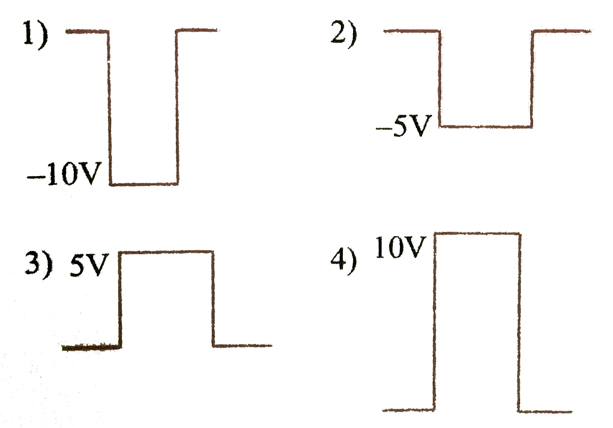 .02:56View Solution
For the circuit shown in figure, Find
(1) the output voltage ,
(2) the voltage drop across series resistance ,
(3) the current through Zener diode.
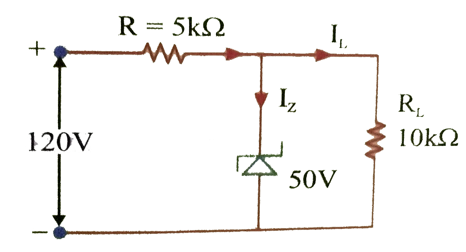 .04:37View Solution
Current amplification factor of a common base configuration is `0.88`. Find the value of base current when the emitter current is `1 m A`.
01:48View SolutionIn a transistor, the emitter circuit resistance is `100 Omega` and the collector resistance is `100 Omega`. The power gain. If the emitter and collector currents are as sumed ton be equal, will be.
01:04View SolutionFrom the output characteristics of common emitter circuit shown in Fig., calculate the value of `beta_(ac)` and `beta_(dc)` of the transistor when `V_(cE)` is `10 V` and `I_c =4.0mA`.
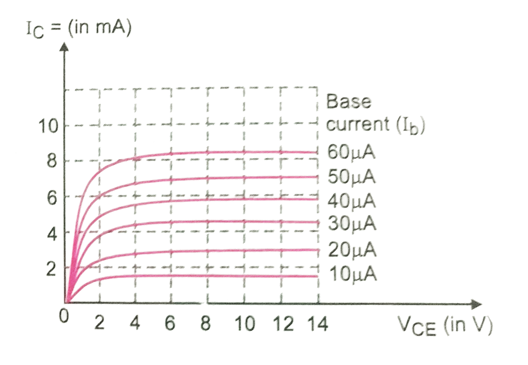 04:02View Solution
In common emitter transistor as shown in Fig., the `V_(BB)` supply can be varied from 0 V to 5.0V. The Si. Transistor has `beta_(ac)=250` and `R_(B)=100kOmega, R_(c)=1k Omega,V_(C C)=5.0V`. Assume that when the transistor is saturated, `V_(CE)=0V` and `V_(BE)=0.8V`. Calculate the minimum base current, for which the transistor will reach saturation. Hence, determine `V_(i)` when the transistor is 'switched on' find ranges of `V_(i)` for which the transistor is switched off and switched on.
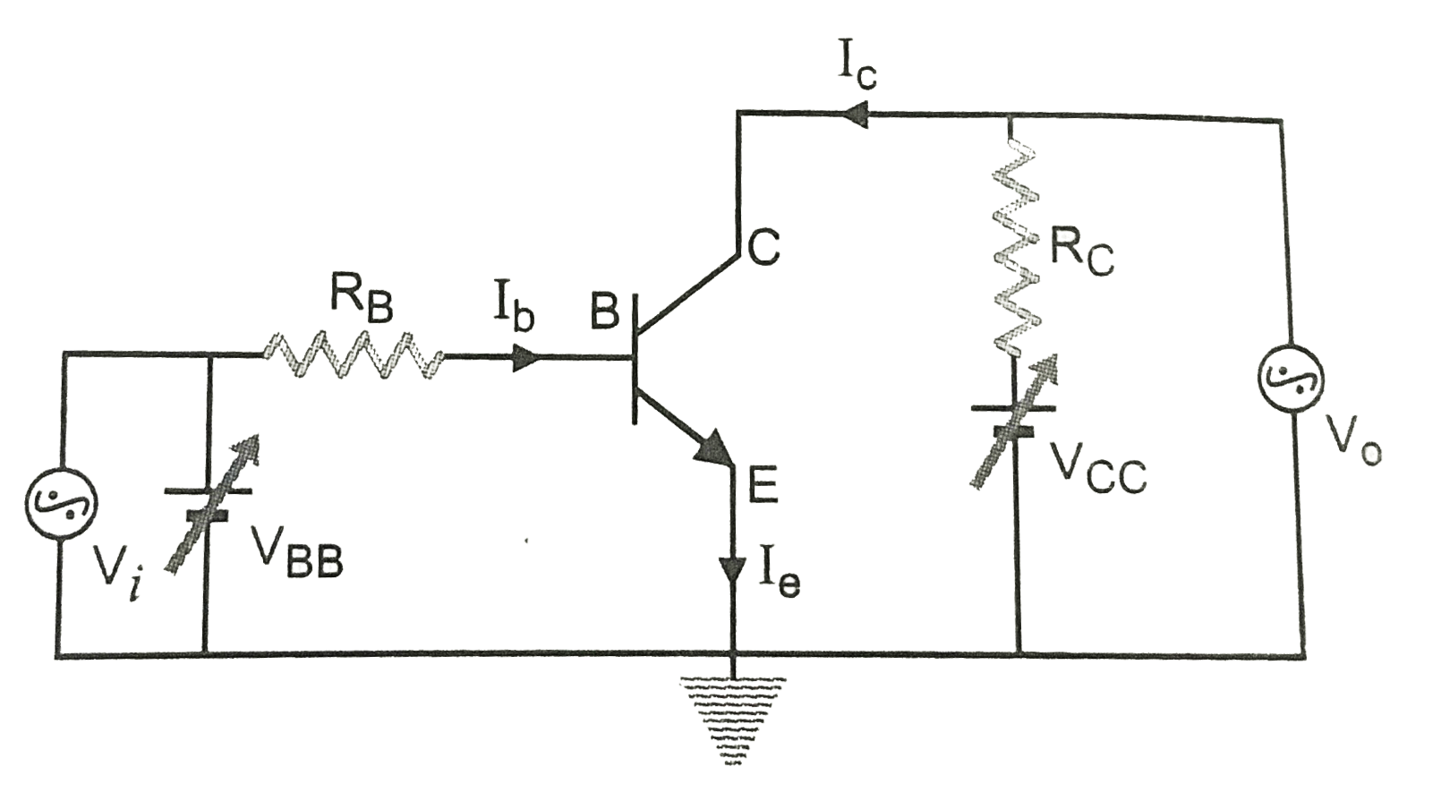 08:36View Solution
Two amplifiers are connected one after the other in series (cascaded). The first amplifier has a voltage gain of 10 and the second has a voltage gain of 20 . If the input signal is 0.01 V , calcualte the output AC signal .
02:36View SolutionIn a single state transistor amplifier, when the signal changes by `0.02 V` the base current by `10 mu A` and collector current by `1 mA`. If collector load `R_(C) = 2k Omega` and `R_(L) = 10 k Omega`, Calculate :
(i) Current Gain
(ii) Input Impedance,
(iii) Effective `AC` load,
(iv) Voltage gain and
(v) Power gain.04:40View SolutionAn n-p-n transistor in a common - emitter mode is used as a simple voltage amplifier with a collector current of 4 mA. The positive terminal of a 8 V battery is connected to the collector through a load resistance ` R_L ` and to the base through a resistance ` R_B ` . The collector - emitter voltage ` V_(CE) = 4 V` , the base - emitter voltage ` V_(BE) = 0.6 V` and the current amplification factor ` beta = 100 ` . Calculate the values of ` R_L ` and `R_B` .
05:18View SolutionIn a negative feedback amplifier, the gain without feedback in `100`, feed back ratio is `1//25` and input voltage is `50 m V`. Calculate
(i) gain with feedback
(ii) feedback factor
(iii) output voltage
(iv) feedback voltage
(v) new input voltage so that output voltage with feedback equals the output voltage without feedback.03:44View SolutionConvert binary number `10111` into decimal number.
01:43View SolutionThe Boolean expression of the output `Y` of the inputs `A` and `B` for the circuit shown in the fig.
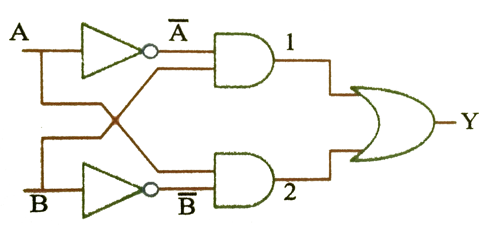 .01:57View Solution
The diagram of a logic circuit is given below. The output `F` of the circuit is represented by
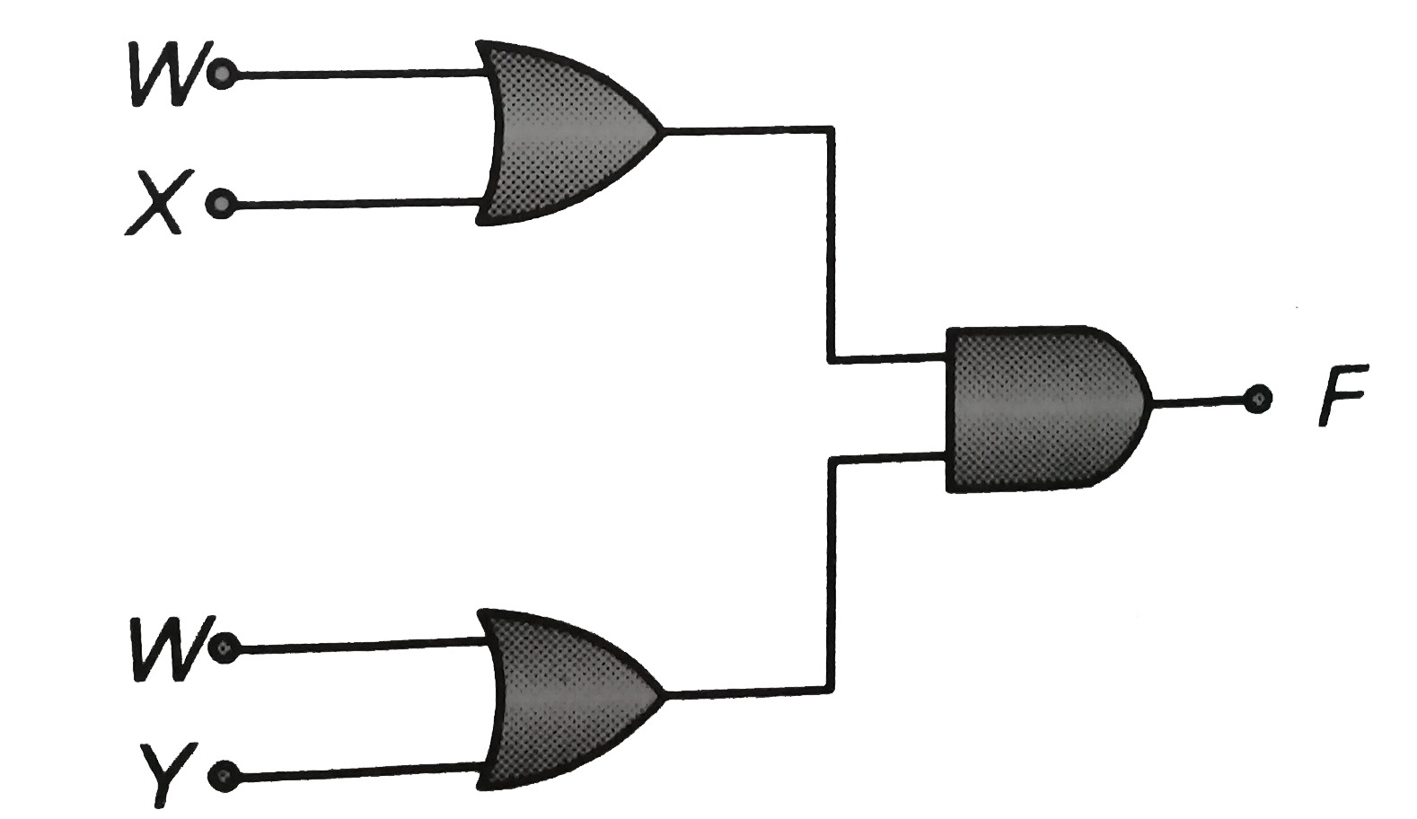 02:19View Solution
The logic circuit and its truth table are given, what is the gate `X` in the diagram
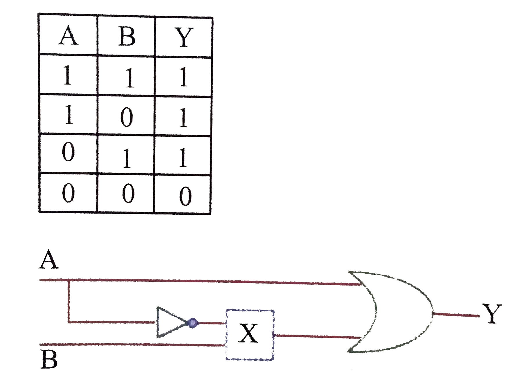 .03:48View Solution
You are given two circuit as shown in Fig.and . Which consists of NAND gates. Identify the logic operation carried out by the two circuits.
 03:40View Solution
Justify the output wavefrom (y) of the OR gate for input and as gives in Fig.
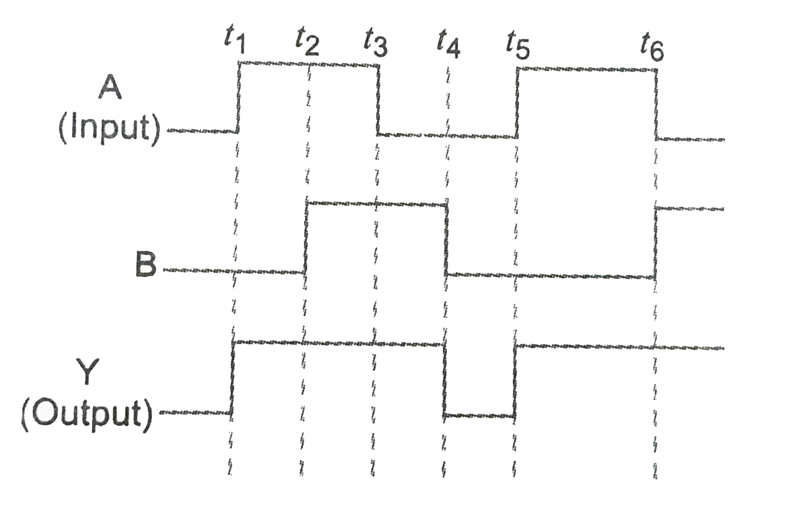 03:58View Solution
Draw logic diagrams for the Boolean expressions given below :
(i) `A * overline B + overline A * B = Y`
(ii) `(A + overline B)* (overline A + B) = Y`.04:17View Solution
Solved Example questions and complete solutions for chapter SEMI CONDUCTOR DEVICES of NARAYANA PHYSICS (HINGLISH) of Class 12
