Complete Solutions to Level-III (C.W) of chapter SEMI CONDUCTOR DEVICES of Class 12 book with complete answers and questions
| Class 12 | PHYSICS |
| Chapter | SEMI CONDUCTOR DEVICES |
| NARAYANA | Level-III (C.W) |
| Number Of Questions | 20 |
| Academic Year | 2023-24 |
If the ratio of the concentration of electron to that of holes in a semiconductor is `(7)/(5)` and the ratio of current is `(7)/(4)` then what is the ratio of their drift velocities ?
01:57View SolutionIf the resistivity of copper is `1.7 xx 10^(-6) Omega cm`, then the mobility of electrons in copper, if each atom of copper contributes one free electron for conduction, is [The amomic weight of copper is `63.54` and its density is `8.96 g//c c]` :
04:30View SolutionA pure silicon crystal of length `l(0.1m)` and area `A(10^(-4) m^(2))` has the mobility of electron `(mu_(e))` and holes `(mu_(h))` as `0.135 m^(2)//Vs` and `0.48 m^(2)//Vs`, respectively, If the voltage applied across it is `2V` and the intrinsic charge concen-tration it is `2V` and the intrinsic charge concen-tration is `n_(i) = 1.5 xx 10^(6) m^(-3)`, then the total current flowing through the crystal is.
04:40View SolutionFind the current produced at room temperature in a pure germanium plate of area `2 xx 10^(-4) m^(2)` and of thickness `1.2 xx 10^(-3) m` when a potential of `5 V` is applied across the faces. Concentration of carries in germanium at room temperature is `1.6 xx 10^(6)` per cubic metre. The mobilities of electrons and holes are `0.4 m^(2) V^(-1) s^(-1)` and `0.2 m^(2) V^(-1) s^(-1)` respectively. The heat energy generated in the plate in `100` second is.
04:37View SolutionAn n-type semiconductor has impurity level `20 meV` below the conduction band. In a thermal collision, transferble enegry is `KT`. The value of `T` for which electrons start to jump in conduction bond is :
01:43View SolutionAssume that the number of hole-electron pair in an intrinsic semiconductor is proportional to `e^(- Delta E//2KT)`. Here `Delta E` = energy gap and `k=8.62 xx 10^(-5) eV//"kelvin"`
The energy gap for silicon is `1.1 eV`. The ratio of electron hole pairs at`300 K` and `400 K` is :04:16View SolutionIn the circuit shown in figure (1), the `V_(0),I_(1),I_(D_(1))`, and `I_(D_(3))` are respectively.
(A)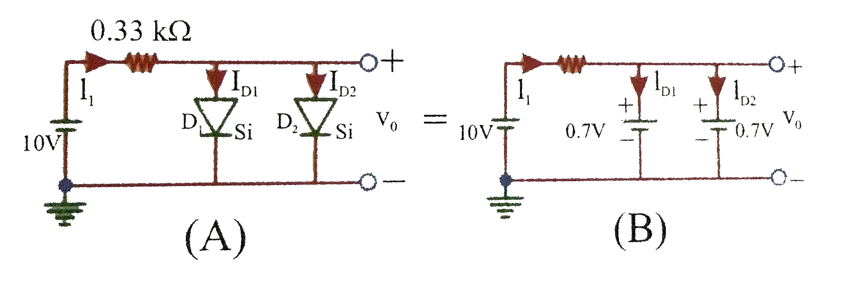 03:45View Solution
For a junction diode, the ratio of forward current `(I_(f))` and reverse current is.
[`I_(e)` = electronic charge,
`V` = voltage applied across junction,
`k` = Boltzmann constant
`T` = temperature in kelvin].01:43View SolutionIn the diagram `D` an ideal diode and an alternating voltage of peak value `10 V` is connected as input `V_(1)`. Which of the following diagram represents the correct wavelength of output voltage `V_(theta)` ?
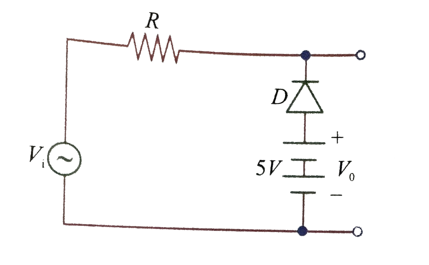 .07:30View Solution
For a `CE`-transistor amplifier, the audio signal voltage across the collector resistance of `2k Omega` is `2V`. Suppose the current amplification factor of the transistor is `100`. Find the input signal voltage and base current, if the base resistance is `1 k Omega`.
02:14View SolutionIn the cuircuit shown here the transistor used has a current gain `beta=100`. What should be the bias resistor `R_(BE)` so that `V_(CE)=5V("neglect "V_(BE))`
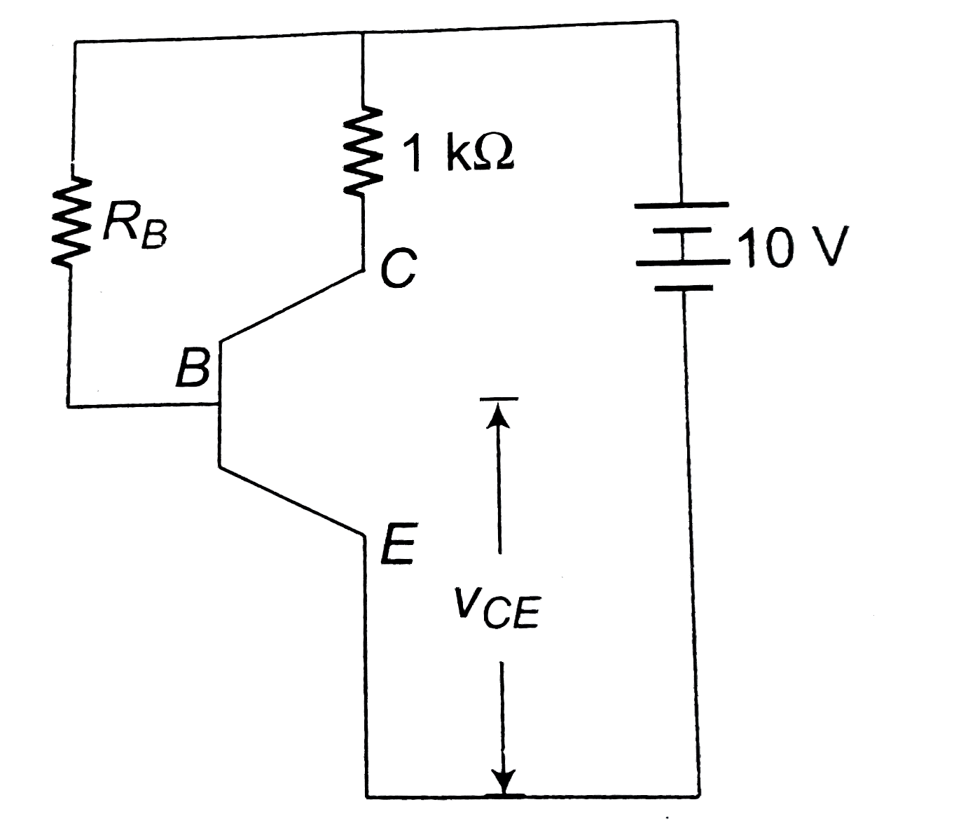 04:01View Solution
An n - p- n transistor is connected in common - emitter configuraration in which collector supply is 8 V and the voltage drop across the load resistance of ` 800 Omega ` connected in the collector circuit is 0.8 V . If current amplification factor is 25 , determine collector - emitter voltage and base current . If the internal resistance of the transistor is ` 200 Omega ` , calculate the voltage gain and the power gain.
06:27View SolutionFor a `CE` transistor amplifier, the audio signal voltage across the collector resistance of `2k Omega` is `2V`. Suppose the current amplification factor of the transistor is `100`. The value of `R_(B)` in series with `V_(BB)` supply of `2V`, if the `DC` base current has to be `10` times the signal current is.
03:24View SolutionFigure shows the transfer characteristics of a base biased `CE` transistor. Which of the following statements are true ?
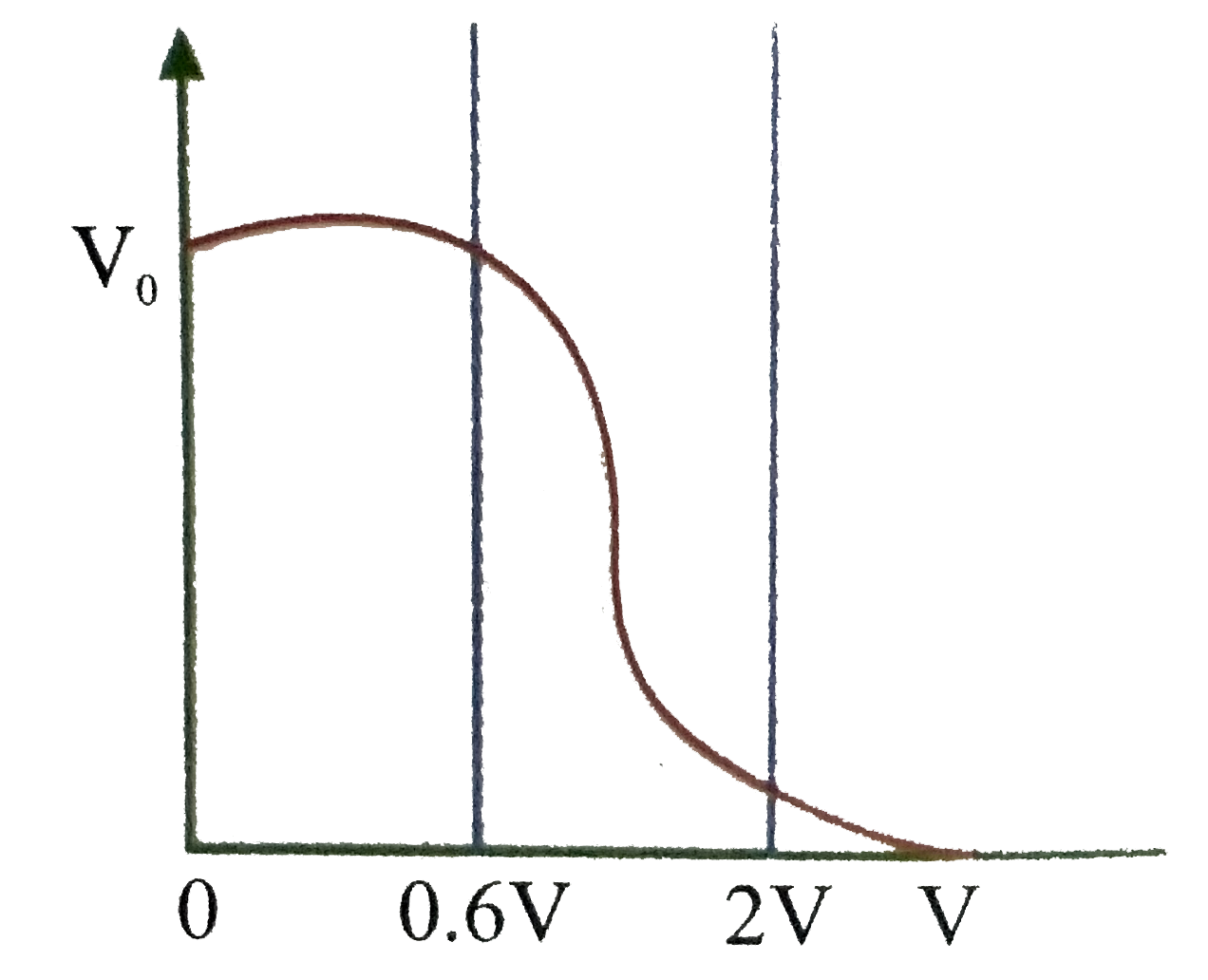
(A) At `V_(1) = 0.14 V` transistors is in active state
(B) At `V_(1) = 1V` it can be used as an amplifier
(C) At `V_(1) = 0.5 V`, it can be used as a switch turned off
(D) At `V_(1) = 2.5 V`, it can be used as switch turned on05:07View SolutionThe following configuration of gate is equivalent to
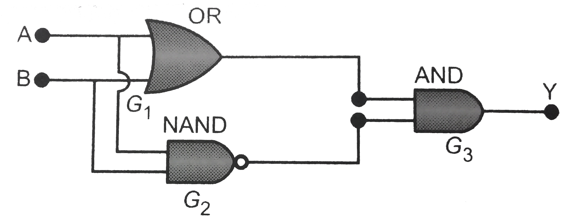 02:36View Solution
The combination of the gates shown below produces
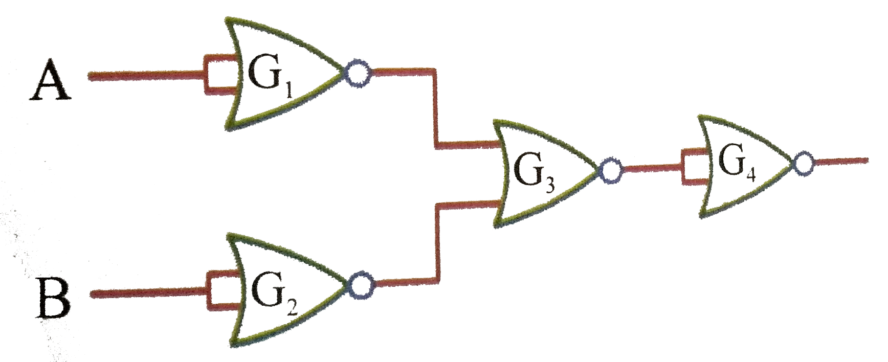 .02:29View Solution
Which of the following truth tables is true ?
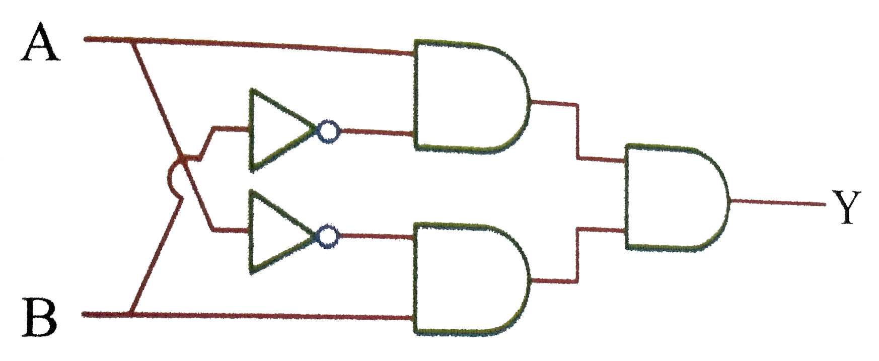 .02:49View Solution
Truth table for system of four `NAND` gates as shown in figure is :
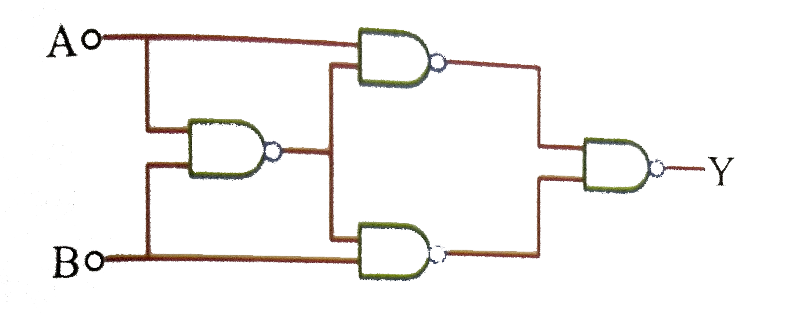 .04:02View Solution
The logic circuit shown below has the input waveforms 'A' and 'B' as shown. Pick out the correct output waveform
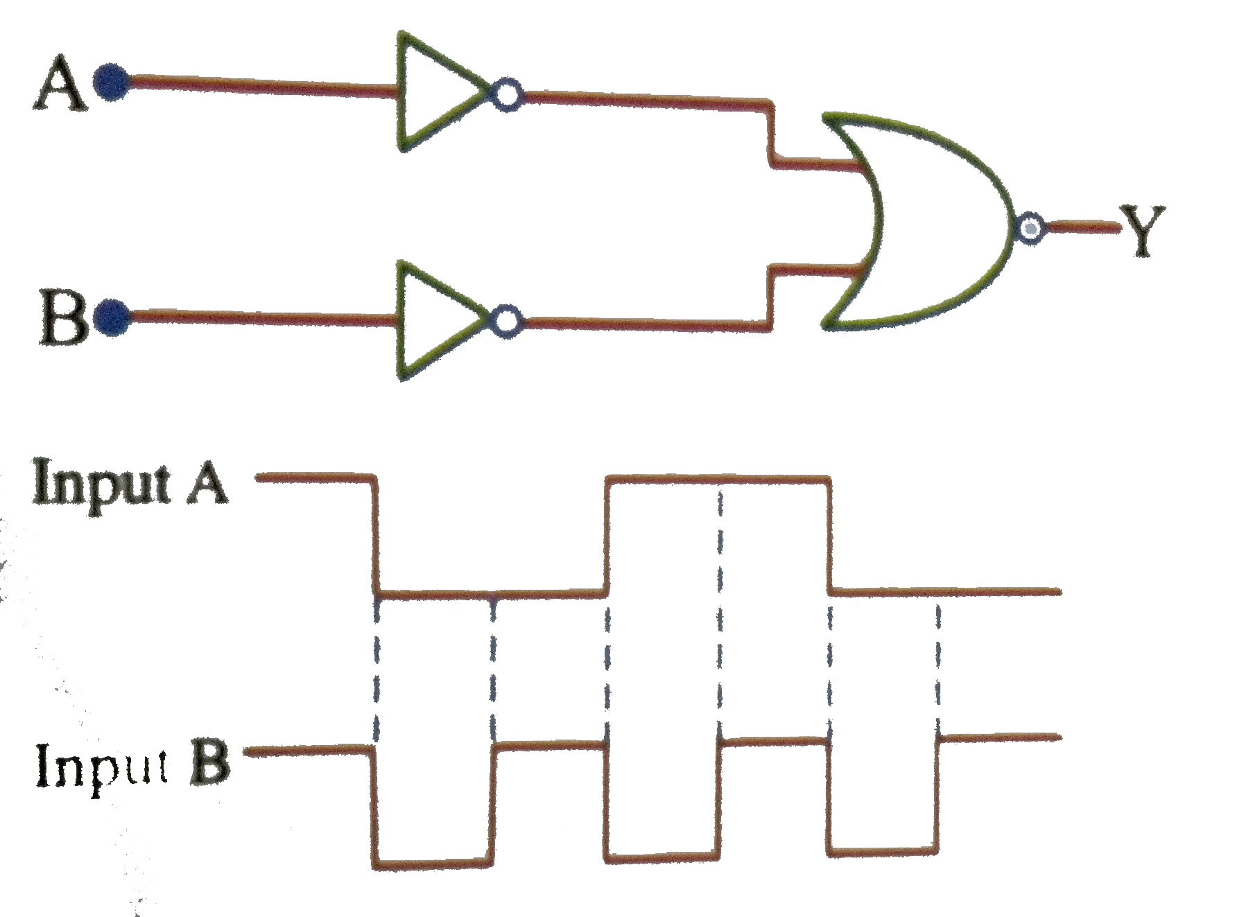 .03:28View Solution
Logic gates `X` and `Y` have the truth tables shown below

`{:(P,Q,R,P,R),(0,0,0,0,1),(1,0,0,1,0),(0,1,0,,),(1,1,1,,):}`
When the output of `X` is connected to the input of `Y`, the resulting combination is equivalent to a single.02:29View Solution
Level-III (C.W) questions and complete solutions for chapter SEMI CONDUCTOR DEVICES of NARAYANA PHYSICS (HINGLISH) of Class 12
