Complete Solutions to Only One Option is Correct of chapter SEMICONDUCTORS AND ELECTRONIC DEVICES of Class 11 book with complete answers and questions
| Class 11 | PHYSICS |
| Chapter | SEMICONDUCTORS AND ELECTRONIC DEVICES |
| DC PANDEY MASTER PROBLEM PACKAGE | Only One Option is Correct |
| Number Of Questions | 55 |
| Academic Year | 2023-24 |
A `P`-type semiconductor can be obtained by adding
View SolutionThe valance of the impurity atom that is to be added to germanium crystal so as to make it a `N`-type semiconductor, is
View SolutionA piece of copper and the other of germanium are cooled from the room temperature to 80 K, then which of the following would be wrong statements?
View SolutionIn an insulator, the forbidden energy gap between the valence band and conduction band is of the order of
View SolutionThe energy band gap of Si is
View SolutionIn an semiconductor the separation between conduction band and valence band is of the order of
View SolutionA piece of semiconductors is connected in sereis in an electric circuit. On increasing the temperautre, the current in the circuit will
View SolutionIntrinsic semiconductor is electrically neutral. Extrinsic semiconductor having large number of current carriers would be
View SolutionMobilities of electrons and holes in a sample of intrinsic germanium at room temperature are `0.36 m^(2)//Vs` and `0.17 m^(2)//Vs`. The electron and hole densities are each equal to `2.5 xx 10^(19) m^(-3)`. The electrical conductivity of germanium is.
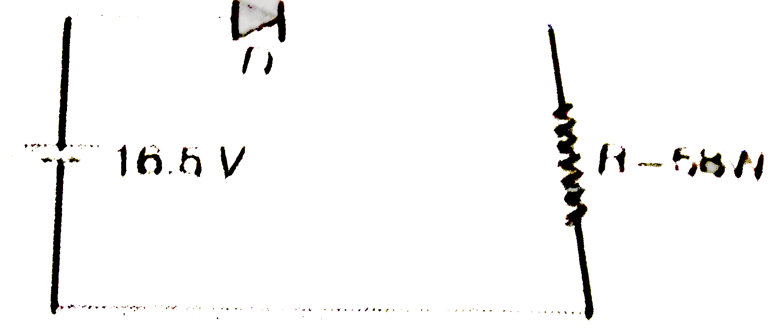
View SolutionIn the circuit given below, the value of the current is

View SolutionWhat is the current in the circuit shown below?

View SolutionIn a p-n junction depletion region has a thickness of the order of
View SolutionFor the given circuit of `PN`-junction diode, which of the following statements is correct?
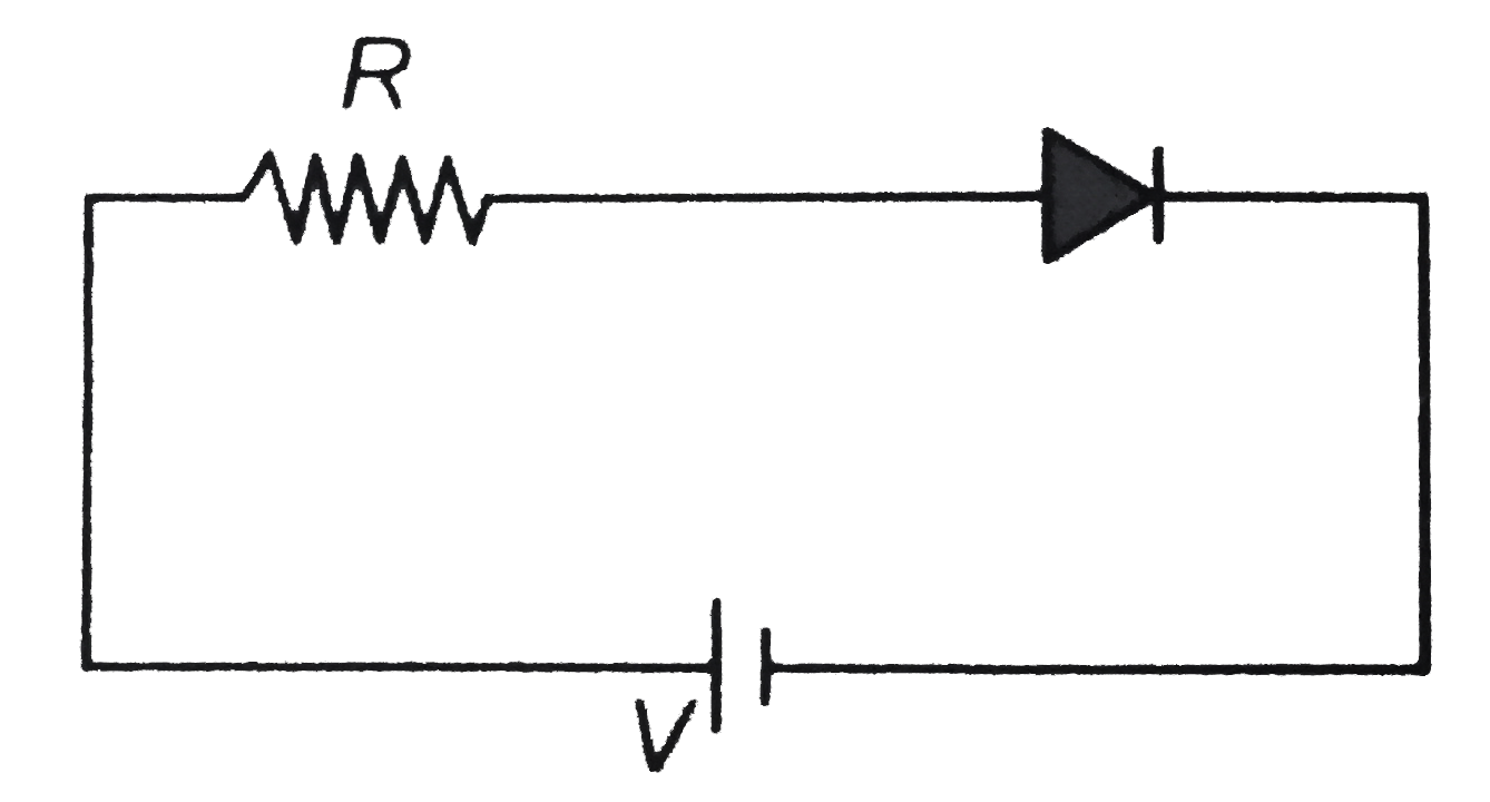
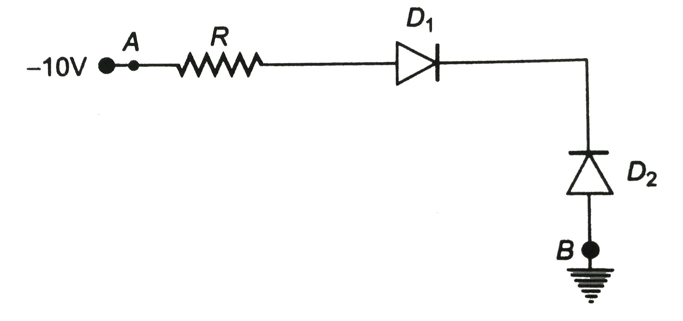
View SolutionThe diode shown in the circuit is a silicon diode. The potential difference between the points `A` and `B` will be
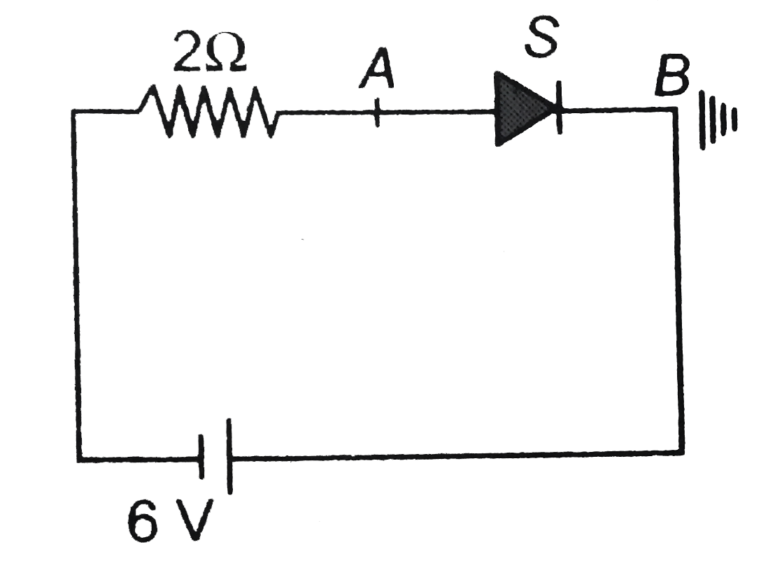
View SolutionThe current through an ideal `PN`-junction shown in the following circuit diagram will be
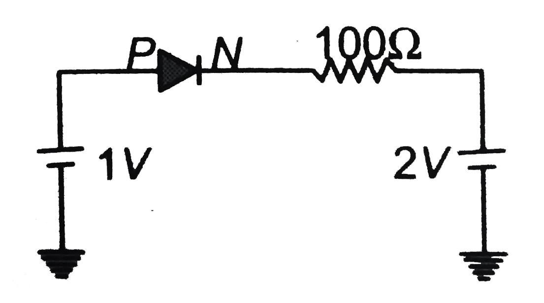
View SolutionIn the given figure, which of the diodes are forward biased?
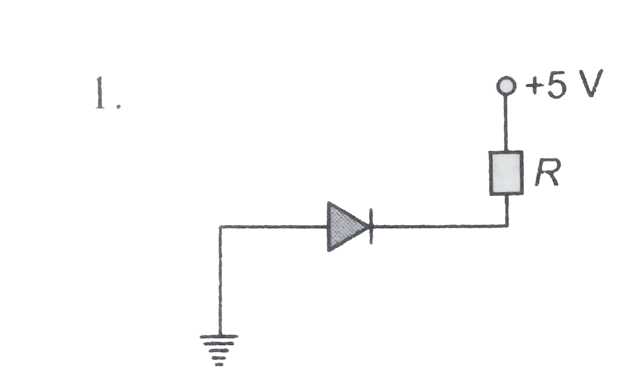
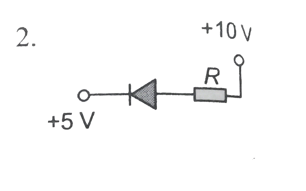
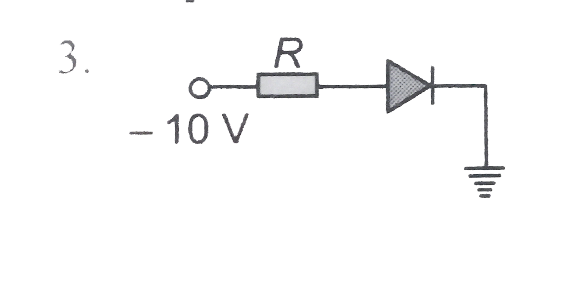
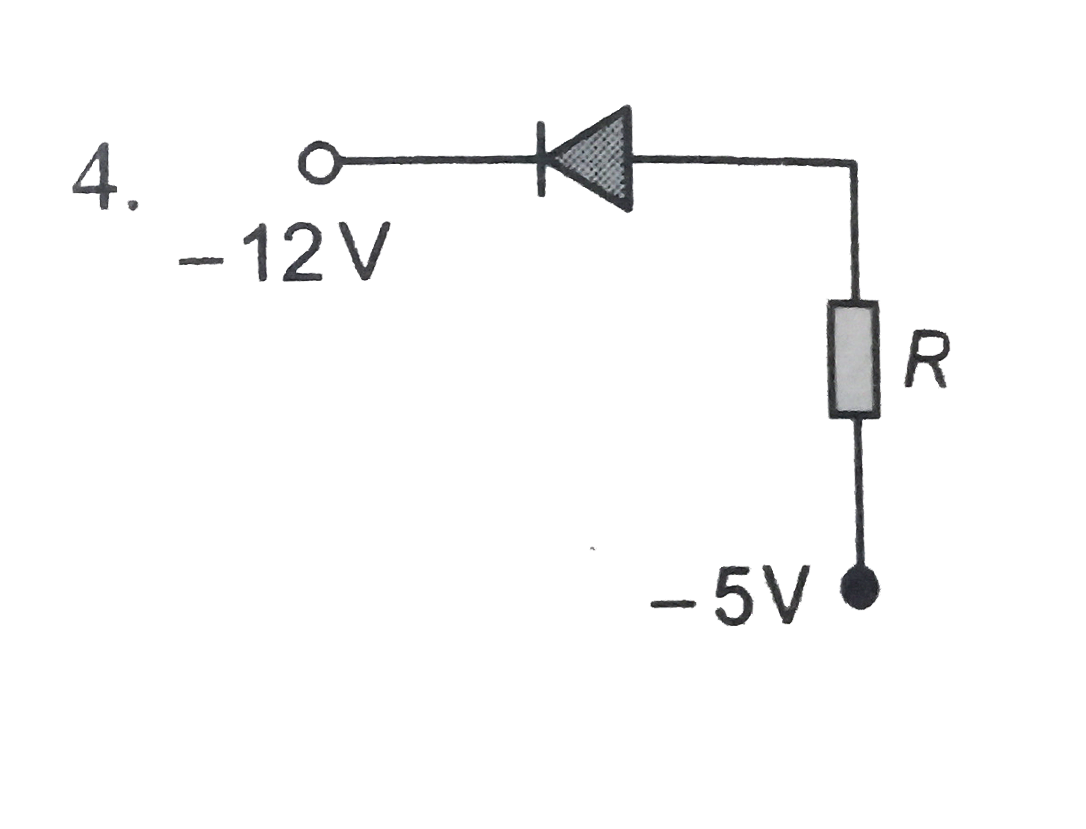
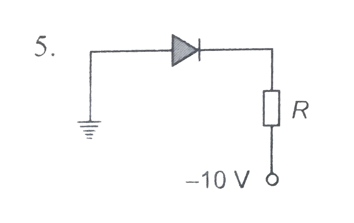
View SolutionThe equivalent resistance of the circuit across `AB` is given by
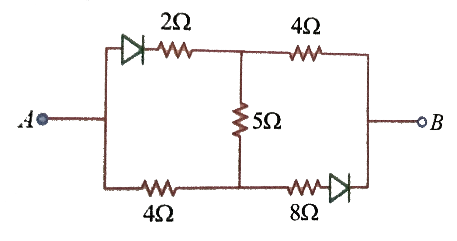 .
.
View SolutionThe width of depletion region in p-n junction diode is `500 nm` and an intrinsic electric field of `6xx 10^(5) Vm^(-1)` is also found to exist in it. What is the kinetic energy which a conduction electron must have in order to diffuse from the n-side to p-side?
View SolutionThe Boolen expression for the circuit given in figure is

View SolutionThe Boolen expression for the circuit given in figure is

View SolutionIn the case of constant `alpha` and `beta` of a transistor
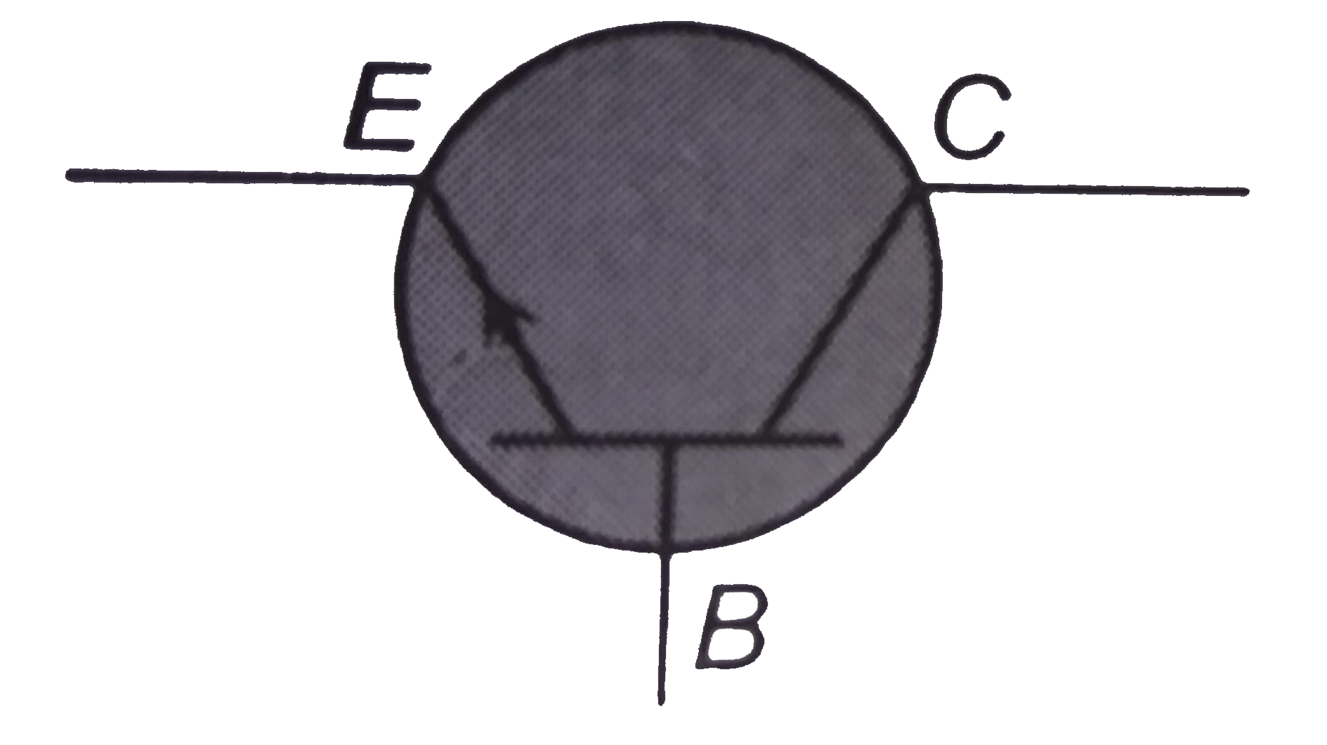
View SolutionThe symbol given in figure represents
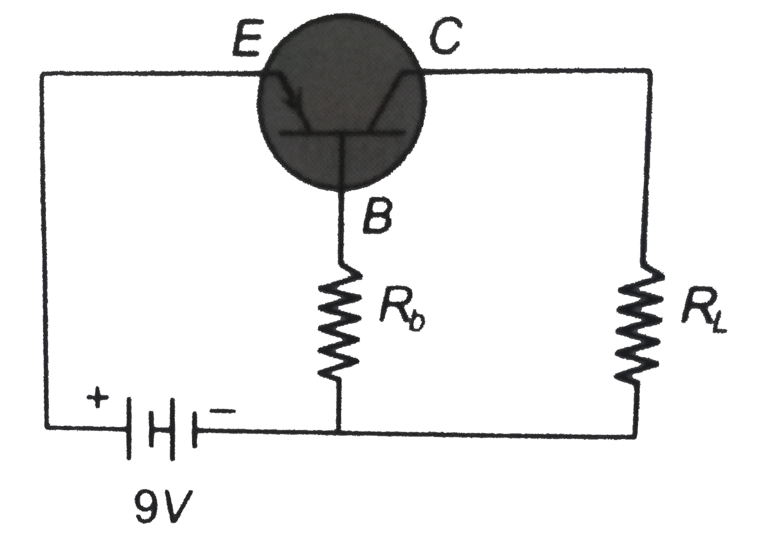
View SolutionIn a transistor circuit shown here the base current is `35 muA`. The value of the resistor `R_(b)` is
View SolutionIn a common base transistor circuit, the current gain is 0.98. On changing the emitter current by 5.00 mA, the change in collector current is
View SolutionThe transfer ration of a transistor is `50`. The input resistance of the transistor when used in the common -emitter configuration is `1 kOmega`. The peak value for an `A.C.` input voltage of `0.01 V` peak is
View SolutionTo use a transistor as an amplifier
View SolutionA transistor has three impurity regions , emitter , base and collector. Arrange them in order of increasing doping levels.
View SolutionWhat is `beta` value for transistor whose `alpha=0.98`?
View SolutionWhen the emitter current of a transistor is changed by 1 mA, its collector current changes by 0.990 mA. In the common base circuit, current gain for the transistor is
View SolutionChoose the corrector relation between the transistor parameters `alpha` and `beta`.
View SolutionIn a transistor, the current amplification factor `alpha` is 0.9. The transistor is connected in common base configuration. The change in collector current when base current changes by 4 mA is
View SolutionGiven below are four logic gates symbol (figure). Those for OR, NOR and NAND are respectively
View SolutionThe combination of gates shown here are equivalent to
View SolutionGive Boolean expression and Truth table for NOR gate.
View SolutionTo get an output of 1 form the circuit shown in figure the input must be :-
_E01_514_Q01.png)
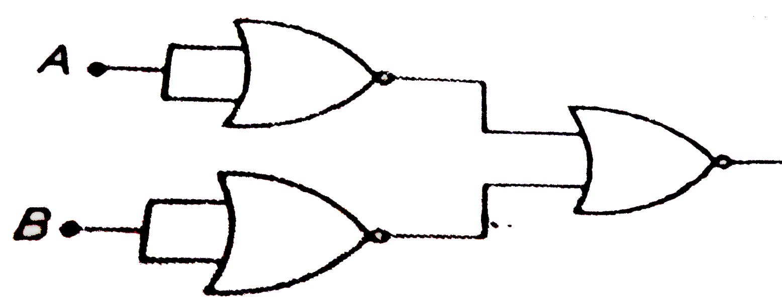
View SolutionThe combination of the gates shown in the figure produces
View SolutionThe following truth table corresponds to the logic gate
`|(A,B,X),(0,0,0),(0,1,1),(1,0,1),(1,1,1)|`
View SolutionThe symbol represents :-
_E01_344_Q01.png)
View SolutionThe conductivity of a semiconductor increases with increase in temperature because
View SolutionIn figure , assuming the diodes to be ideal ,
View SolutionHole is
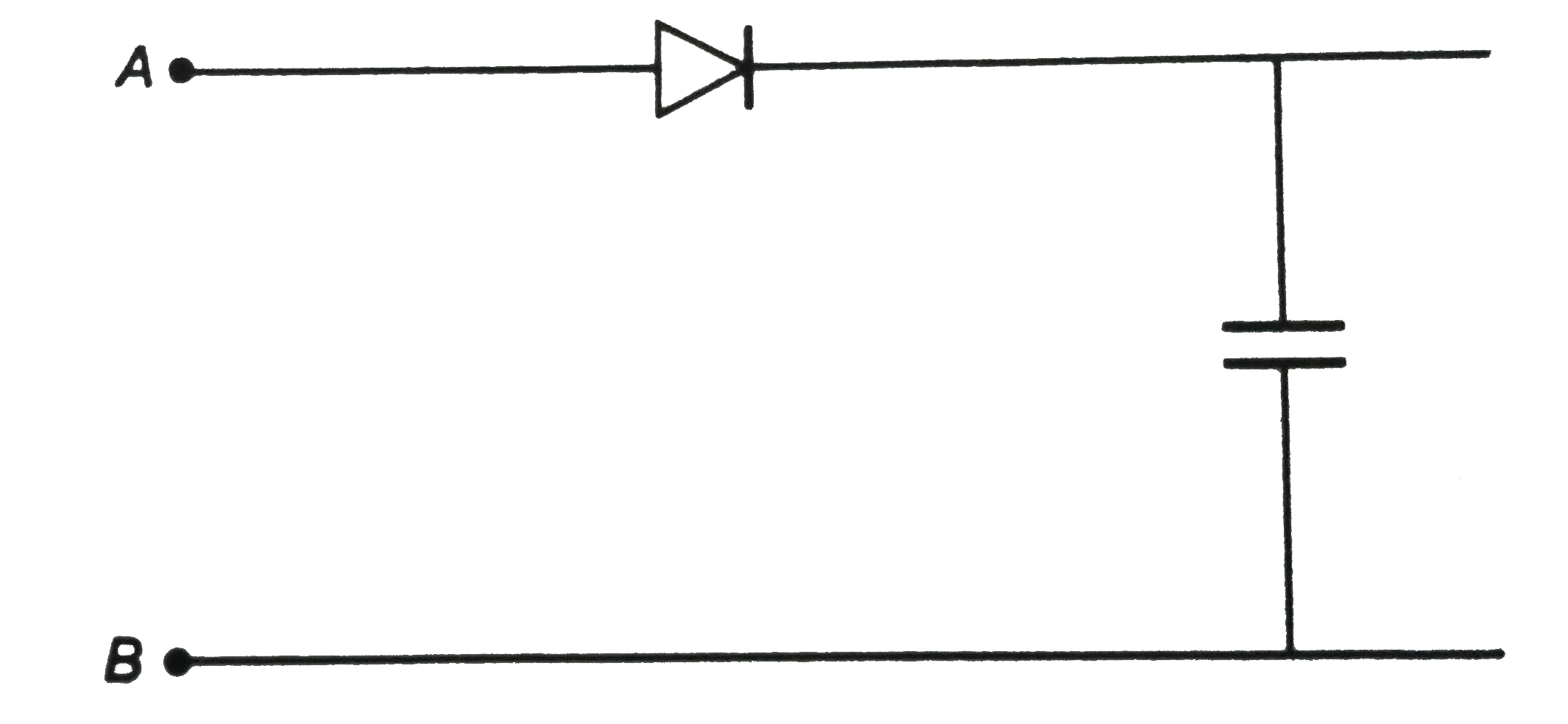
View SolutionA 220 V AC supply is connected between points A and B . What will be the potential difference V across the capacitor ?
View SolutionIn a common emitter transistor, the current gain is `80`. What is the change in collector current, when the change in base current is `250 muA`?
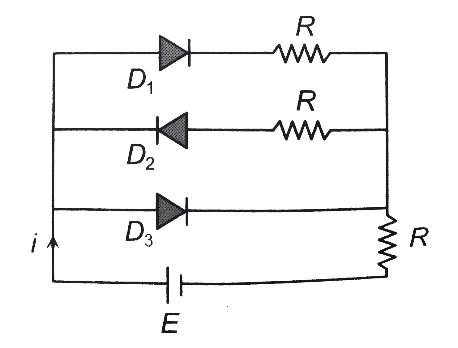
View SolutionIn the following circuit of `PN` junction diodes `D_(1),D_(2)` and `D_(3)` are ideal then `i` is
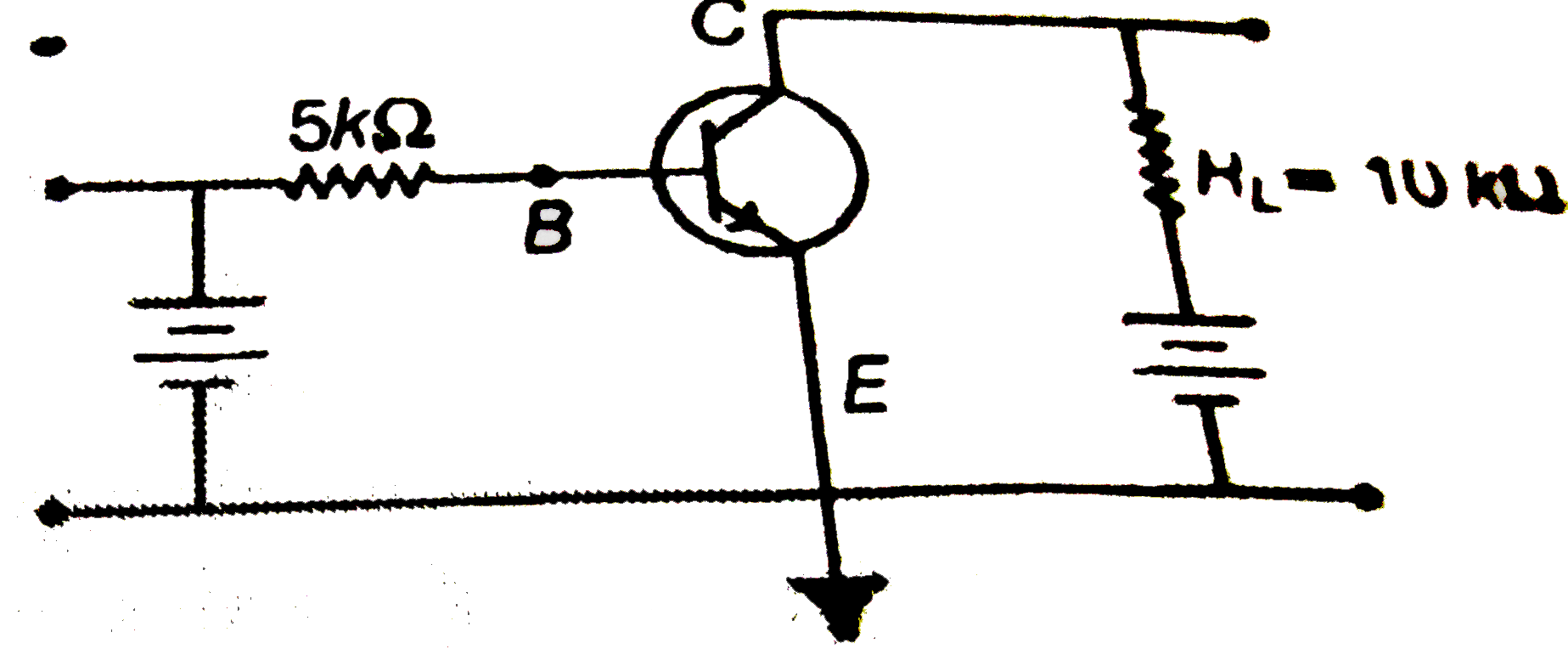
View SolutionThe adjoining diagram shows the biasing of an npn-transistor in common emitter configuration used in an amplifer. The design of the transistor is such that `98%` of the charge carries passing through the emitter reach the collector. If base current changes from `50 muA` to `100muA`, then the corresponding change in the voltage across the load resistance `R_(L)` will be
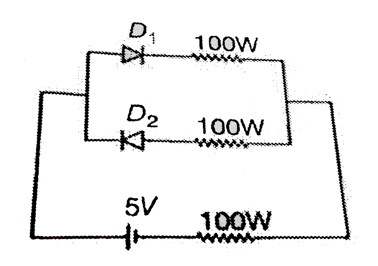
View SolutionTwo ideal diodes `D_(1)` and `D_(2)` are connected with the battery of 5 volt as shown in figure. Then the current through diode `D_(1)` is
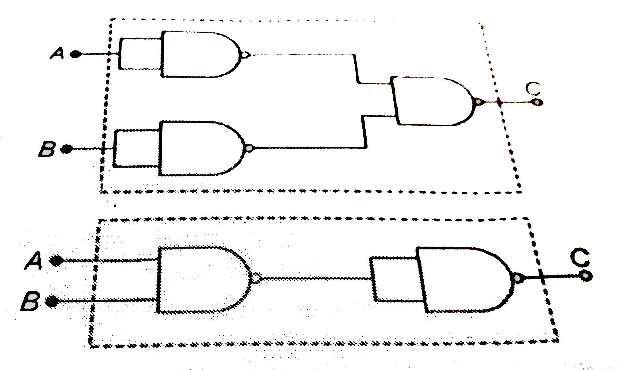
View SolutionWrite the truth table for the circuit given in Fig., consisting of NOR gates only. Identify the logic operations (OR, AND, NOT) performed by two circuits.

View SolutionIn half - wave rectification, what is the output frequency, if the
input frequency is 50 Hz ? What is the output frequency of a full - wave rectifier
for the same input frequency ?
View SolutionThe circuit shown in the figure acts as

View SolutionThe current gain for common emitter amplifier is 69. If the emitter current is `7.0 mA`, find (i) base current and (ii) collector current.
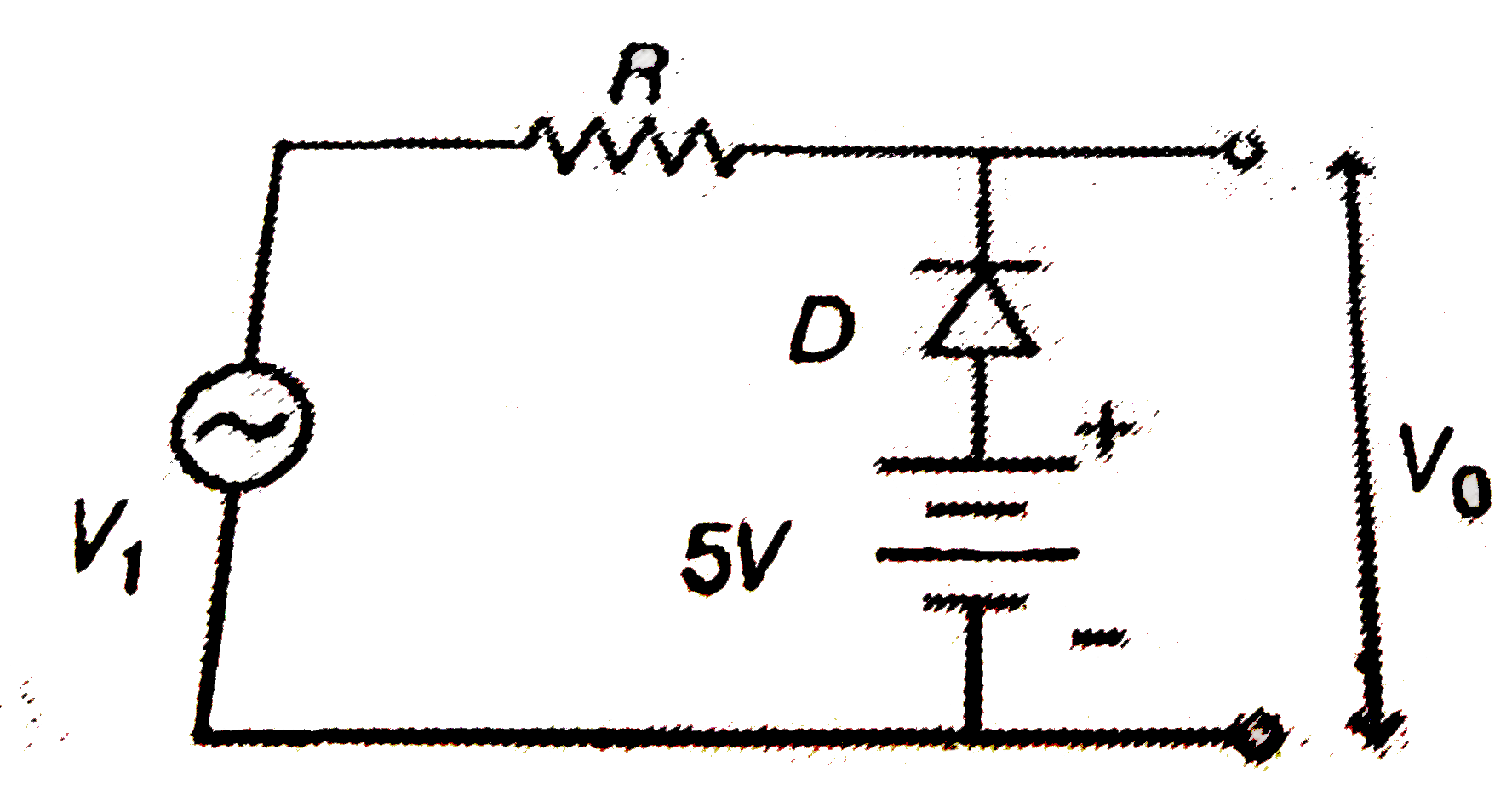
View SolutionIn the figure, D is an ideal diode and an alternating voltage of peak value 10 volts si connected as input `V_(1)`. Which of the following figures represents the correct waveform of output voltage `V_(0)` ?
View SolutionRegarding transistor what is not correct.
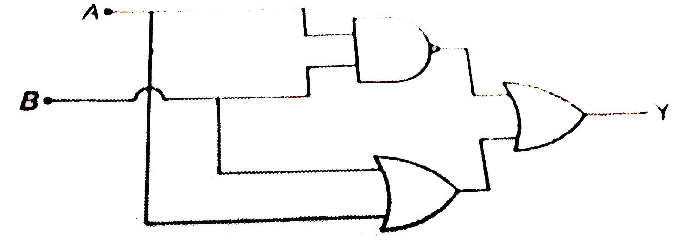
View SolutionThe truth table for the circuit shown in the figure is
View SolutionThe diode D shown in the circuit is governed by the V-I relation `V=(0.7 + 100 I)` Volt. The current supplied by the battery is
View SolutionA sample of n-type silicon
View Solution
Only One Option is Correct questions and complete solutions for chapter SEMICONDUCTORS AND ELECTRONIC DEVICES of DC PANDEY PHYSICS (HINGLISH) of Class 11