Complete Solutions to CBSE Question of chapter SEMICONDUCTORS of Class 12 book with complete answers and questions
| Class 12 | PHYSICS |
| Chapter | SEMICONDUCTORS |
| BANSAL | CBSE Question |
| Number Of Questions | 32 |
| Academic Year | 2023-24 |
How does the width of the depletion layer of a p-n junction diode change with decrease in reverse bias?
02:55View Solution
In the following diagrams, write which of the nodes are forward biased and which are reverse biased.01:47View SolutionThe output of a 2-inputs NAND gate is fed to a NOT gate. Write down the truth table for the output of the combination for all possible input of the combination for all possible inputs of A and B.
02:18View SolutionZENER DIODE AS VOLTAGE REGULATOR
05:26View SolutionDraw a labelled circuit diagram for a common emitter amplifier using n-p-n transistor. Write down the expression for its voltage gain. What is the phase difference between input and output signals?
03:55View Solution
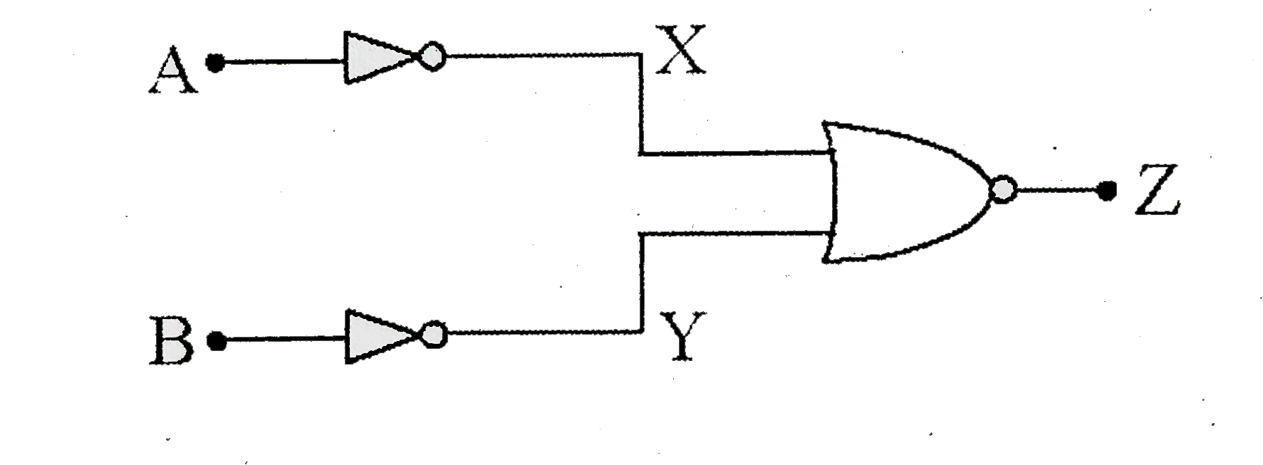
Name of gate obtained from the combination of gates shown in the figure. Draw its logic symbol. Write the truth table of the combination.03:38View SolutionHow is p-type semiconductor formed? Name the major charge carriers in it. Draw the energy band diagram of a p-type semiconductor.
12:47View SolutionZENER DIODE AS VOLTAGE REGULATOR
05:26View SolutionDraw a labelled circuit diagram of a common base amplifier using a p-n-p transistor. Define the term voltage gain and write an expression for it.
08:29View SolutionDraw the voltage current characteristic fo a zener diode.
01:35View SolutionWith the help of a labelled circuit diagram, explain how an n-p-n transistor can be used as an amplifier in common-emitter configuration. Explain how the input and output voltages are out of phase by 1800 for a common-emitter transistor amplifier.
09:51View Solution
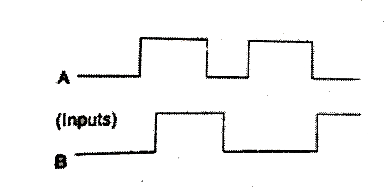
Give the logic symbol for an OR gate. Draw the output wave form for input wave forms A and B for this gate.02:53View SolutionHow does the resistivity of (i) a conductor and (ii) a semiconductor vary with temperature? Give reason for each case.
06:56View SolutionDistinguish between conductor (or metals), semiconductors and insulators on the basis of their energy bands.
02:44View Solution(a). Explains briefly with the help of a circuit diagram how V-I characteristics of a p-n junction diode are obtainedin (i) forward bias, and (ii) reverse bias.
(b). A photo diode is fabricated from a semiconductor with a band gap of 2.8 EV. Can it detect wave length of 6000. nm? Justify.19:12View SolutionExplain (i) forward biasing (ii) reverse biasing of a P-N junction diode. With the help of a circuit diagram, explain the use of this device as a half wave rectifier.
10:29View SolutionDistinguish between conductor (or metals), semiconductors and insulators on the basis of their energy bands.
02:44View Solution
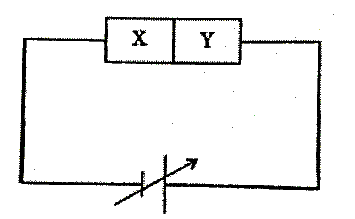
Two semiconductor materials X and Y shown in the given figure, are made by doping germanium crystal with indum and arsenic respectively. The two are joined end to end and connected to a battery as shown.
(i). Will the junction be forward biased or reverse biased.?
(ii). Sketch a V-I graph for this arrangement.03:39View SolutionDraw the circuit diagram of a common emitter amplifier using n-p-n transistor. What is the phase difference between the input signal and output voltage? State two reasons why a common emitter amplifier is preferred to a common base amplifier.
11:24View SolutionExpalin the formation of energy band in solids. Draw energy band diagram for (i) and conductor (ii) and intrinsic semiconductor.
04:26View SolutionDistinguish between intrinsic semiconductor and p-type semiconductor. Give reason, why a p-type semiconductor crystal is electrically neutral, although `n_(h)gt gtn_(e)`?
06:18View Solution
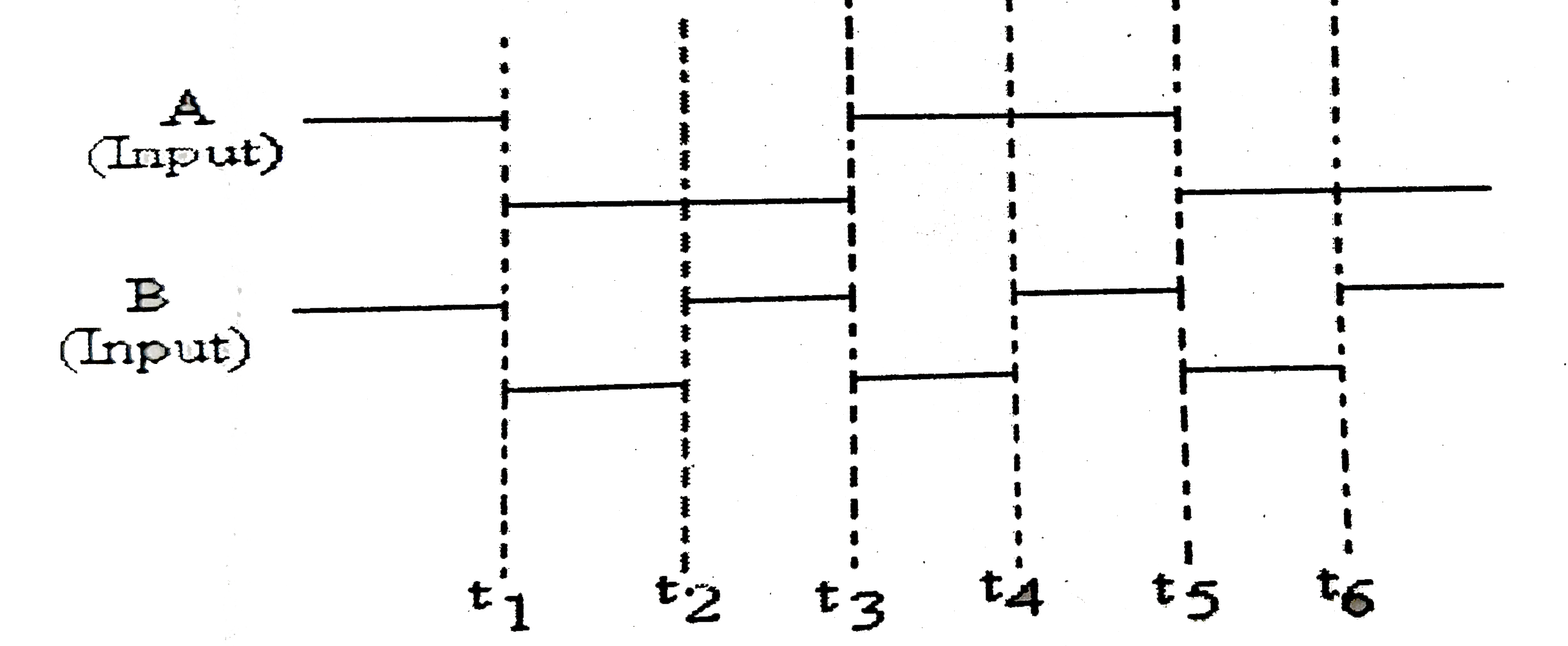
The give inputs A, B are fed to a 2-input NAND gate. Draw the output wave form of the gate.04:08View SolutionThe output of a 2-input AND gate is fed to a NOT gate. Give the name of the combination and its logic symbol. Write down its truth table.
02:59View SolutionDraw a circuit diagram of a transistor amplifier in CE configuration. Define the terms (i) Input resistance and (ii) Current amplification factor. How are these determined using input and output characteristics?
09:34View SolutionExplain (i) forward biasing (ii) reverse biasing of a P-N junction diode. With the help of a circuit diagram, explain the use of this device as a half wave rectifier.
10:29View SolutionIn V-I characteristics of a p-n junction diode, why is the current under reverse bias almost independent of the applied potential upto a critical voltage?
03:22View Solution(i) Identify the logic gates marked P and Q in the given logic circuit Fig.

(ii) Write down the output at X for the inputs `A=0, B=0` and `A=1, B=1`.02:23View SolutionWhat happens to the width of depletion layer of a p-n junction when it is (i) forward biased, (ii) reverse biased?
04:42View SolutionDraw a circuit diagram of a full-wave rectifier. Explain its working principle. Draw the input/output wave forms indicating clearly the function of the two diode used.
09:40View Solution
You are given a circuit below. Write its truth table. Hence, identify the logic operation carried out by this circuit. Draw the logic symbol of the gate it corresponds to.03:53View SolutionExplain the formation of depletion layer and potential barrier in p-n junction.
Draw the circuit diagram of a half wave rectifier and explain its working.15:26View SolutionDraw a circuit diagram of a full-wave rectifier. Explain its working principle. Draw the input/output wave forms indicating clearly the function of the two diode used.
09:40View Solution
CBSE Question questions and complete solutions for chapter SEMICONDUCTORS of BANSAL PHYSICS (HINGLISH) of Class 12
