Complete Solutions to C.U.Q of chapter SEMI CONDUCTOR DEVICES of Class 12 book with complete answers and questions
| Class 12 | PHYSICS |
| Chapter | SEMI CONDUCTOR DEVICES |
| NARAYANA | C.U.Q |
| Number Of Questions | 100 |
| Academic Year | 2023-24 |
Which property makes the crystalline solids to have sharp melting point ?
View SolutionWhich of the following is not a property of crystalline substance
View SolutionA piece of copper and another of germanium are cooled from room temperature to `80 K`. The resistance of
View SolutionThe difference in the variation of resistance with temperature in a metal and a semiconductor arises essentially due to the difference in the
View SolutionThe manifestation of band structure in solids is due to
View SolutionA solid which is not transperent to visible light and whose conductivily increase with temperature is formed by
View SolutionTo a germanium sample, traces of gallium are added as an impurity. The resultant sample would behave like
View SolutionIn semiconductors at a room temperature
View SolutionIdentify the property which is not characteristic for a semiconductor ?
View SolutionCarbon , silicon and germanium have four valence electrons each . At room temperature which one of the following statements is most appropriate ?
View SolutionThe relation between number of free electrons `(n)` in a semiconductor and temperature `(T)` is given by
View SolutionAn electrically neutral semiconductor has
View SolutionThere is no hole current in conductors because they have
View SolutionIn the insulators
View SolutionIn semiconductors the for bidden energy gap between `V.B` and `C.B` is of the order of
View SolutionThe level formed due to impurity atom, in the for hidden energy gap, very near to the valence band in a p-type semiconductor is called
View SolutionThe bond in semiconductors is
View SolutionOn increasing temperature, the conductivity of pure semiconductors
View SolutionThe mobility of free electrons is greater then that of free holes because
View SolutionA semiconductor at `0 K` behaves as
View SolutionCarbon , silicon and germanium have four valence elcectrons each . These are characterised by valence and conduction bands separated by energy band - gap respectively equal to ` (E_g)_(c) (E_g)_(si) ` and ` (E_g)_(Ge) `. Which of the following statements ture ?
View SolutionThe valency of impurity element for making p-type semiconductors is
View SolutionIn n-type semiconductors the electron concentration is equal to
View SolutionWhich of the following statements is not true ?
View Solutionp-type semiconductor is
View Solutionn-type semiconductor is
View SolutionAn electric field is applied across a semiconductor. Let `n` be the number of charge carries. As temperature increases, `n` will
View SolutionIn a n-type semiconductor, the femi energy level lies
View SolutionAn n-type and p-type silicon can be obtained by doping pure silicon with.
View SolutionThe width of forbidden gap in silicon crystal is `1.2 ev`. When the crystal is converted into a n-type semiconductor the distance of fermi level from conduction band is Greater than `0.55 eV`
View SolutionIn extrinsic semiconductors
View SolutionThe element that can be used as acceptor impurity to dope silicon is
View SolutionAmong the following, the wrong statement on the case of semiconductor is
View SolutionThe value indicated by fermi energy level in an intrinsic semiconductor is
View SolutionThe conduction band and valency band of a good conductors are
View SolutionTwo pieces one of germinium and the other of aluminium are cooled from `T_(1) K` to `T_(2) K`. The resistance of
View SolutionIn intrinsic semiconductor at room temperature the no. of electrons and holes are
View SolutionBand gap in insulator is of the order
View SolutionIn p-type semiconductor conduction in due to
View SolutionIn an intrinsic semiconductor, the fermi energy level is
View SolutionWith increase in temperature in an intrinsic semiconductor the ration of conduction electrons and holes is
View SolutionTo obtain n-type extrinsic semiconductor, the impurity element to be added to germanium should be of valency
View SolutionThe majority carries in a p-type semiconductor are….
View SolutionThe objective of adding impurities in the extrinsic semiconductor is
View SolutionIn intrinsic semiconductor conductivity is
View SolutionIn intrinsic semiconductor conductivity is due to.
View SolutionWhen the conductivity of a semiconductor is only due to breaking of covalent bonds, the semi conductor is called.
View SolutionAssertion (A) : `C,Si` and `Ge` have `4` Valancy each both but `C` is an insulator where as `Si` and `Ge` are semi conductors
Reason `( R)` : Energy gap is least for `Ge`, less for `Si` compared to `C`, So that free electrons for conduction in `Ge` and `Si` are significant but negligible small for `C`.
View SolutionThe potential barrier at `PN` junction is due to
View SolutionA `PN` junction diode cannot be used
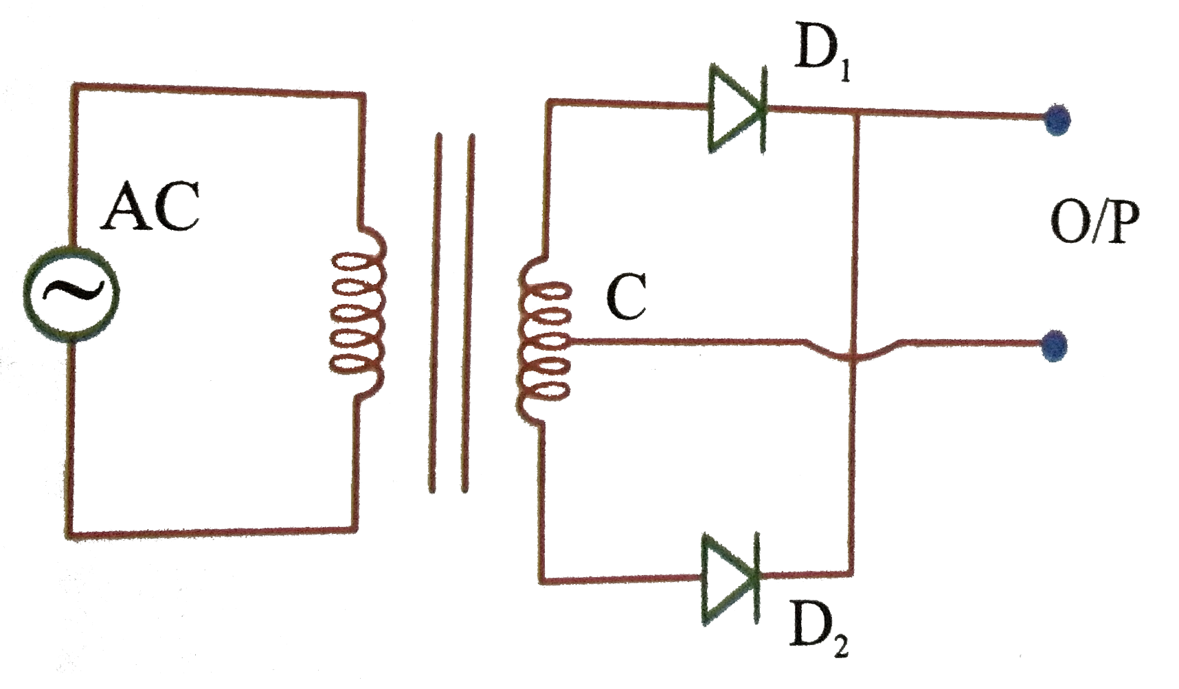
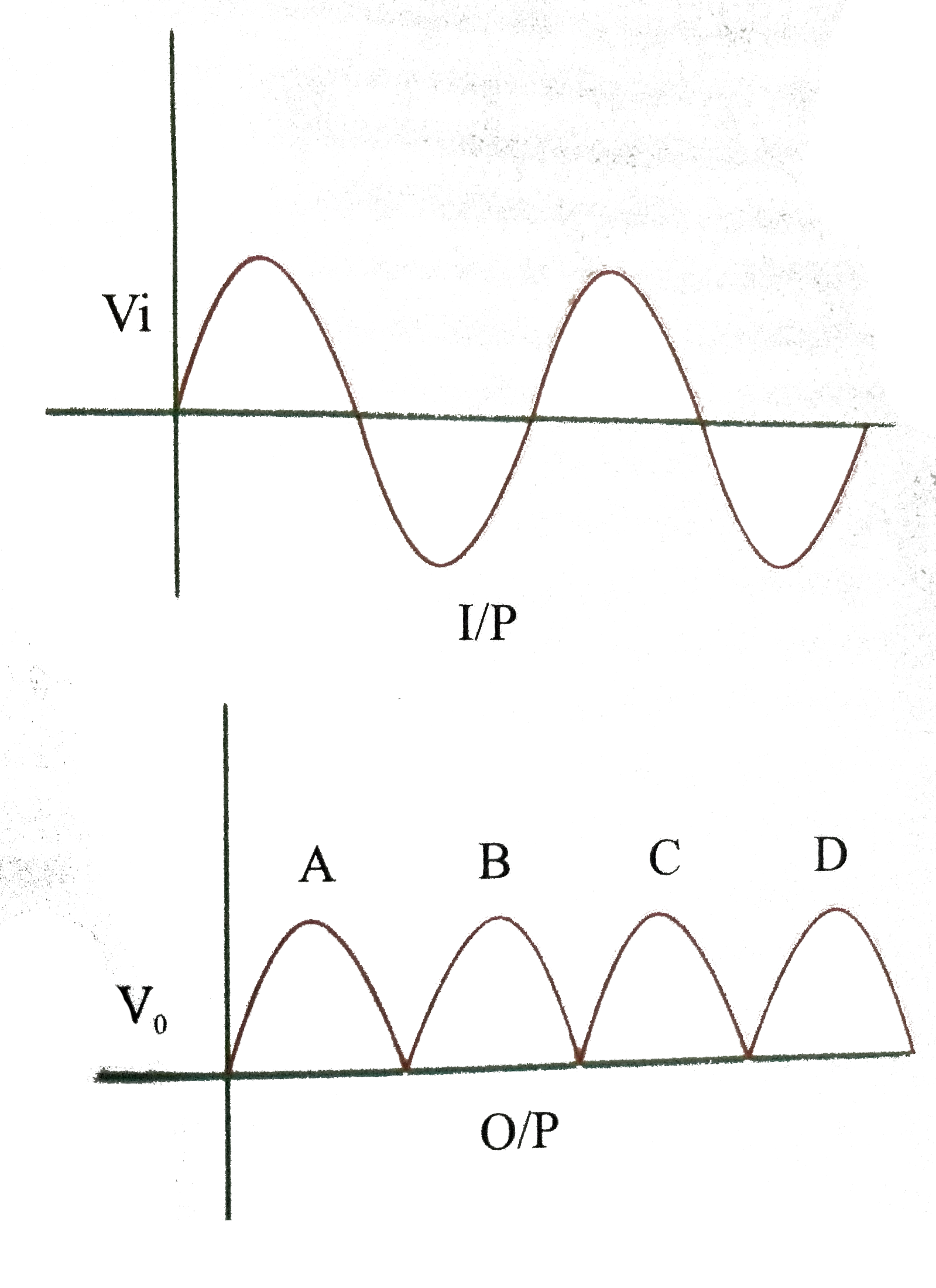
View SolutionA full wave rectifier with the output is shown in fig. the contributions from the diode (2) are.
 .
.

View SolutionA full-wave rectifier is used to convert 'n' `HZ a.c` into `d.c`, then the number of pulses per second present in the rectified voltage is.
View SolutionIf the input frequency of half-wave rectifier is `n Hz ac`, then its output is
View Solution`p-n` junction diode acts as
View SolutionThe process of converting alternating current into direct current is known as
View SolutionOn increasing reverse voltage in a `p-n` junction diode the value of reverse current will
View SolutionIn forward bias the depletion layer behaves like
View Solution`p-n` junction in reverse bias behaves like
View SolutionThe main cause of avalence breakdown is
View SolutionThe main cause of Zener breakdown is.
View SolutionWhen `p-n` junction is forward biased, the current across the junction is mainly due to
View SolutionThe current through any `p-n` junction is due to
(a) drift of charge carriers
(b) diffusion of charge carriers
( c) different concentrations of same type of charge carriers in different regions.
(d) Same concentrations of same type of charge carriers in different regions
View SolutionThe thickness of depletion layer is approximately
View SolutionThe depletion region is
View SolutionDiffusion current in a p-n junction is greater than the drift current in magnitude
View SolutionGermanium diode.
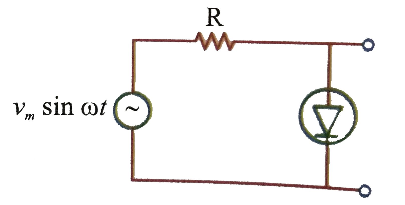
View SolutionThe output of the given circuit in Fig.
 .
.
View SolutionDiode is forward biased and the applied voltage is greater than the potential barrier then
(I) resistance of the junction in the forward bias decreases
(II) potential barrier remains same
(III) width barrier remains decreases
(IV) p-type is at higher potential than the n-type.
View SolutionWhen a junction diode is reverse biased, then current called drift current is due to
View SolutionAmong the following one statement is not correct when a junction diode is forward bias
View SolutionConsidering `a.p-n` junction as a capacitor, forward with `p` and `n` material acting as thin metal electrodes and depletion layer width acting as seperation between them. Basing on this assume that a `n-p-n` transistor is working as an amplifier in `CE` configuration. If `C_(1)` and `C_(2)` are base-emiter and collector emitter junction capacitances, then :
View SolutionConsider the following statements `A` and `B` and identify the correct answer
(1) : Germanium is preferred over silicon in the construction of zener diode.
(2) : Germanium has high thermal stability than silicon in the construction of Zener diode.
View SolutionA Zener diode when used as a voltage regulator is connected
(a) in forward bias
(b) in reverse bias
( c) in parallel to the load
(d) in series to the load.
View SolutionConsider the following statements `A` and `B` and identify the correct answer
(A) A Zener diode is always connected in reverse bias to use it as voltage regulator.
(B) The potential barrier of a `p-n` junction lies between `0.1` to `0.3 V`, approximately.
View SolutionConsider the following statement `A` and `B` and identify the correct choice of the given answers
`A:` The width of the depletion layer in a `P-N` junction diode increases in forwards biase
`B:` In an intrinsic semiconductor the fermi energy level is exactely in the middle of the forbidden gap
View SolutionThe potential in the depletion layer due to.
View SolutionPickout the incorrect statement regarding reverse saturation current in the `p-n` junction diode.
View SolutionWhen the `p-n` junction diode is reverse biased, the thickness of the depletion layer
View Solution`p-n` junction diode can be used as
View SolutionA `p-n` junction diode is reverse biased. Then
View SolutionIn the middle of the depletion layer of a reverse - biased `p - n ` junction , the
View SolutionWhen `p-n` junction diode is forward biased then
View SolutionIn a `p-n` junction photo cell, the value of the photo electromotive force produced by monochromatic light is proportional to
View SolutionThere is a sudden increase in current in zener diode is
View SolutionApplication of a forward biase to a `p-n` junction:
View SolutionIn a p- n junction diode not connected to any circuit,
View SolutionSelect the correct statement from the following :
View SolutionWhen a `PN` juction diode is forwards biased, energy is released at the juction due to the recombination of electrons and holes. This energy is in
View SolutionA `Si` and a `Ge` diode has identical physical dimensions. The band gap in `Si` is larger than that in `Ge`. An indentical reverse bias is applied across the diodes.
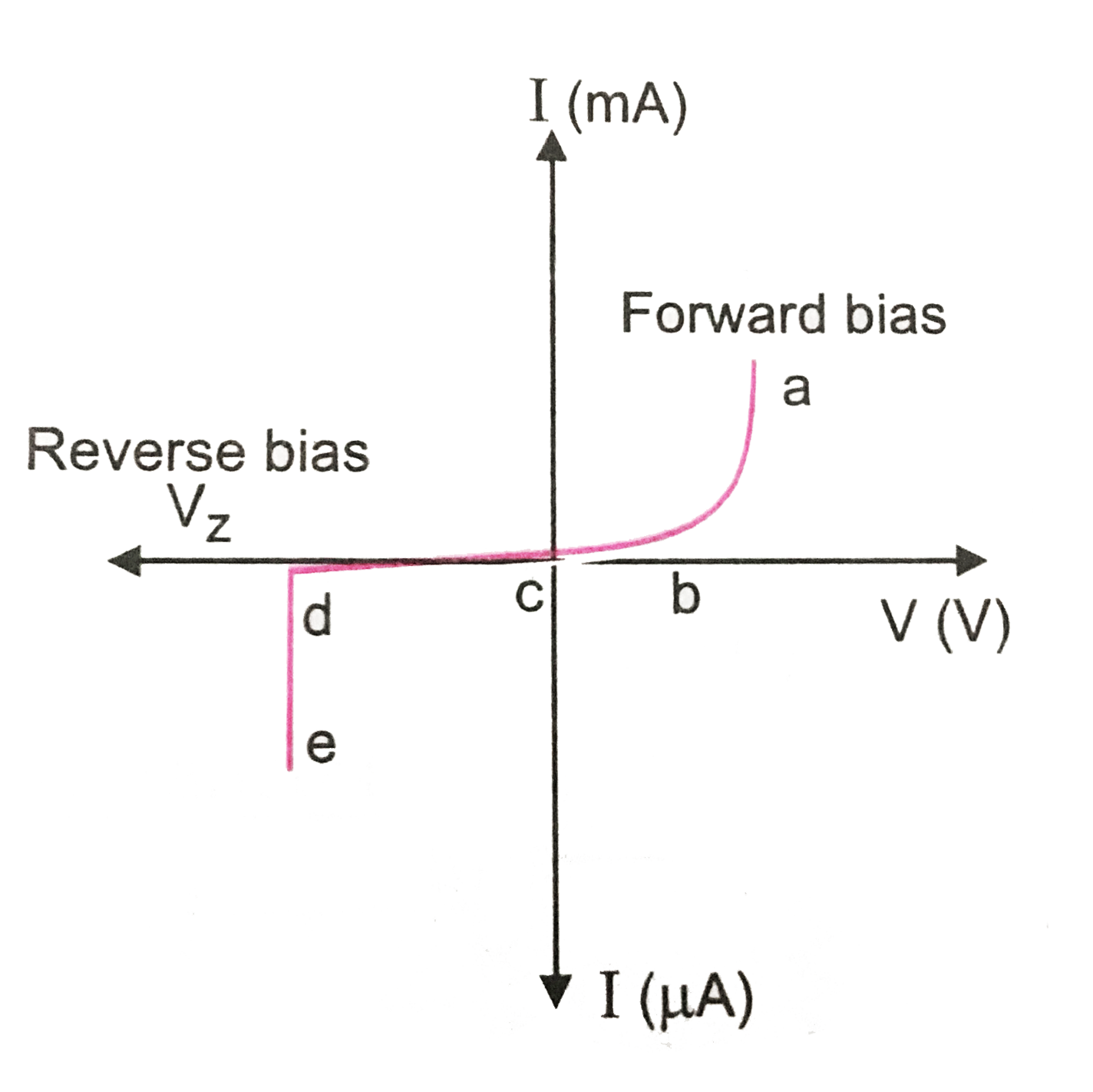
View SolutionThe graph shown in Fig. represents the I-V characteristics of a zener diode. Which part of the characteristics curve is most relevent for its operation as a voltage regular?

View SolutionAssertion (A) : `Si` and `GaAs` are preferred materials for solar cells
Reason (R ) : Energy gap of `Si` is `1.1 eV` and that of `GaAs` is `1.53 eV` which gives maximum irradiance where as other materials like `CdS` or `CdSe (E_(g) = 2.4 eV)` and `PbS (E_(g) = 0.4 eV)` given minimum irradiance.
View SolutionAssertion (A) : Putting p-type semiconductor slabs directly in physical contact can not form `p-n` junction
Reason ( R) : The roughness at contact will be much more than inter atomic crystal spacing `(= 2 Å to 3 Å)` and continuous flow of charge carriers is not possible.
View SolutionAssertion (A) : Eventhough forward bias is known to be more `(mA)` than the current in the reverse bias `(mu A)`, photodiodes are still used in reverse bias.
Reason ( R) : The fractional change in majority charge carriers woulb be much less than that in minority charge carriers due to photo-effects so that minority carrier reverse bias current is more easily to measure with photo diodes than majority carrier forward current.
View SolutionThe correct relation between current gains `alpha` and `beta` is
View SolutionTransistors are made of.
View SolutionIn `n-p-n` transistor the arrow head on emitter represents that the convantional current flows from
View SolutionIn a junction transistor the emitter, base and collector are made of.
View SolutionIn a transistor.
View SolutionIn a transistor
View SolutionIn transistor the emitter current is.
View Solution
C.U.Q questions and complete solutions for chapter SEMI CONDUCTOR DEVICES of NARAYANA PHYSICS (HINGLISH) of Class 12