Complete Solutions to Level-II (C.W) of chapter SEMI CONDUCTOR DEVICES of Class 12 book with complete answers and questions
| Class 12 | PHYSICS |
| Chapter | SEMI CONDUCTOR DEVICES |
| NARAYANA | Level-II (C.W) |
| Number Of Questions | 33 |
| Academic Year | 2023-24 |
Mobilities of electrons and holes in a sample of intrinsic germanium at room temperature are `0.36 m^(2)//Vs` and `0.17 m^(2)//Vs`. The electron and hole densities are each equal to `2.5 xx 10^(19) m^(-3)`. The electrical conductivity of germanium is.
View SolutionIn a `p-n` junction diode the thickness of deplection layer is `2 xx 10^(-6) m` and barrier potential is `0.3 V`. The intensity of the electrical field at the junction is.
View SolutionA potential barrier `V` volts exists across a `P-N` junction. The thickness of the depletion region is 'd'. An electron with velocity 'v' approches `P-N` junction from N-side. The velocity of the electron acrossing the junction is.
View SolutionIn the following, reverse biased diode is.
View SolutionTwo similar `p-n` junctions can be connected in three different ways as shown in the figure. The two connections across which the potentional difference is same are.
(a)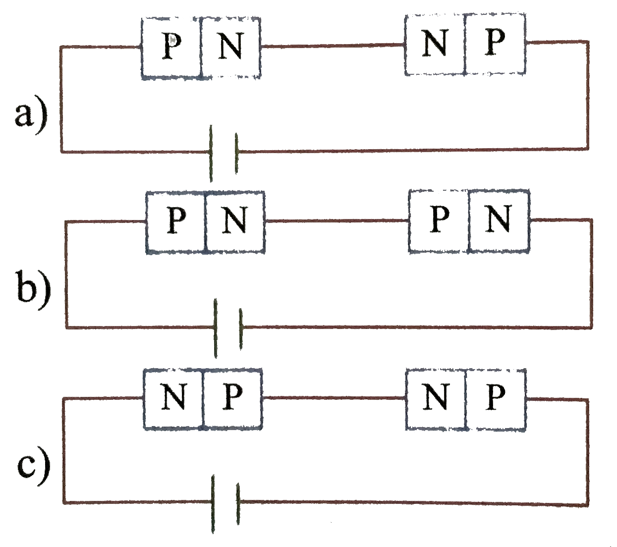
View SolutionIf `V_(1) gt V_(2), r` is resistance offered by diode in forward bias then current through the diode is.
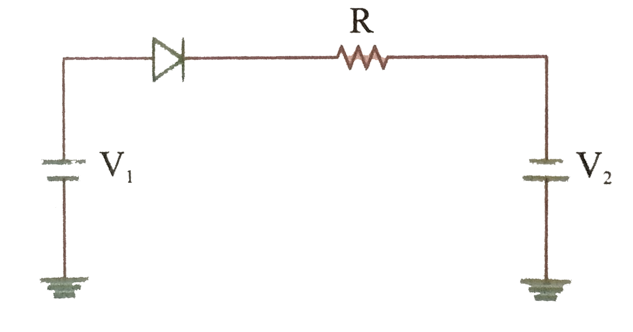 .
.
View SolutionA `PN` junction diode when forward biased has a drop of `0.5 V` which is assumed to be independent of current. The current in excess of `10 mA` through the diode produces large joule heating which damages the diode. If we diode, the resistor used in series with the diode so that the maximum current does not exceed `5 mA` is.
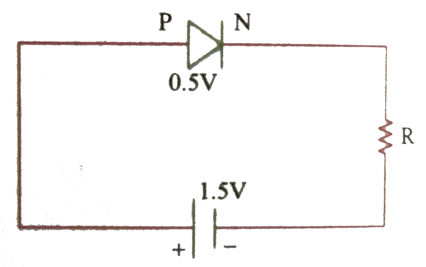 .
.
View SolutionThe circuit shown in figure (1) Contains two diodes each with a forward resistance of `50 ohm` and with infinite reverse resistance. If the battery voltage is `6 V`, the current through the `100 ohm` resistance is.
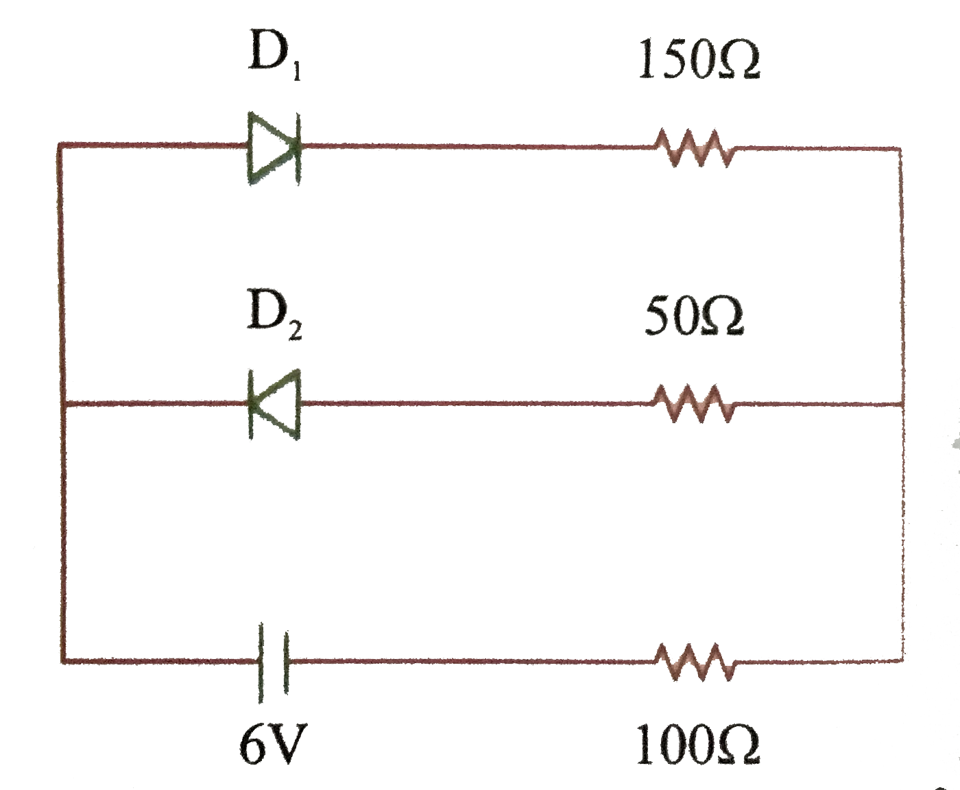 .
.
View Solution`4` ideal diodes are connected as shown in the circuit the current through `50 Omega` is.
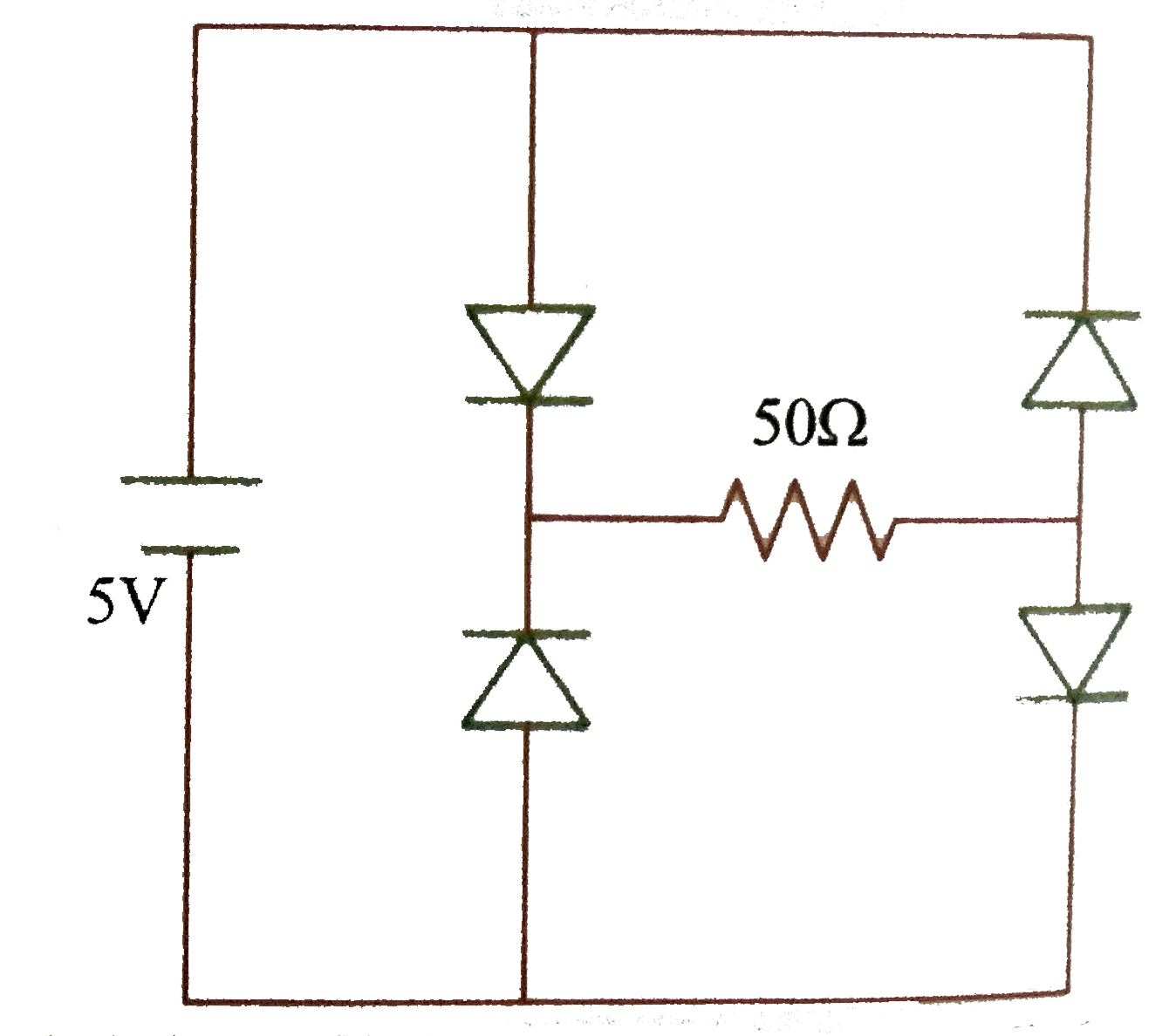 .
.
View SolutionFind the effective resistance between `A` & `B`
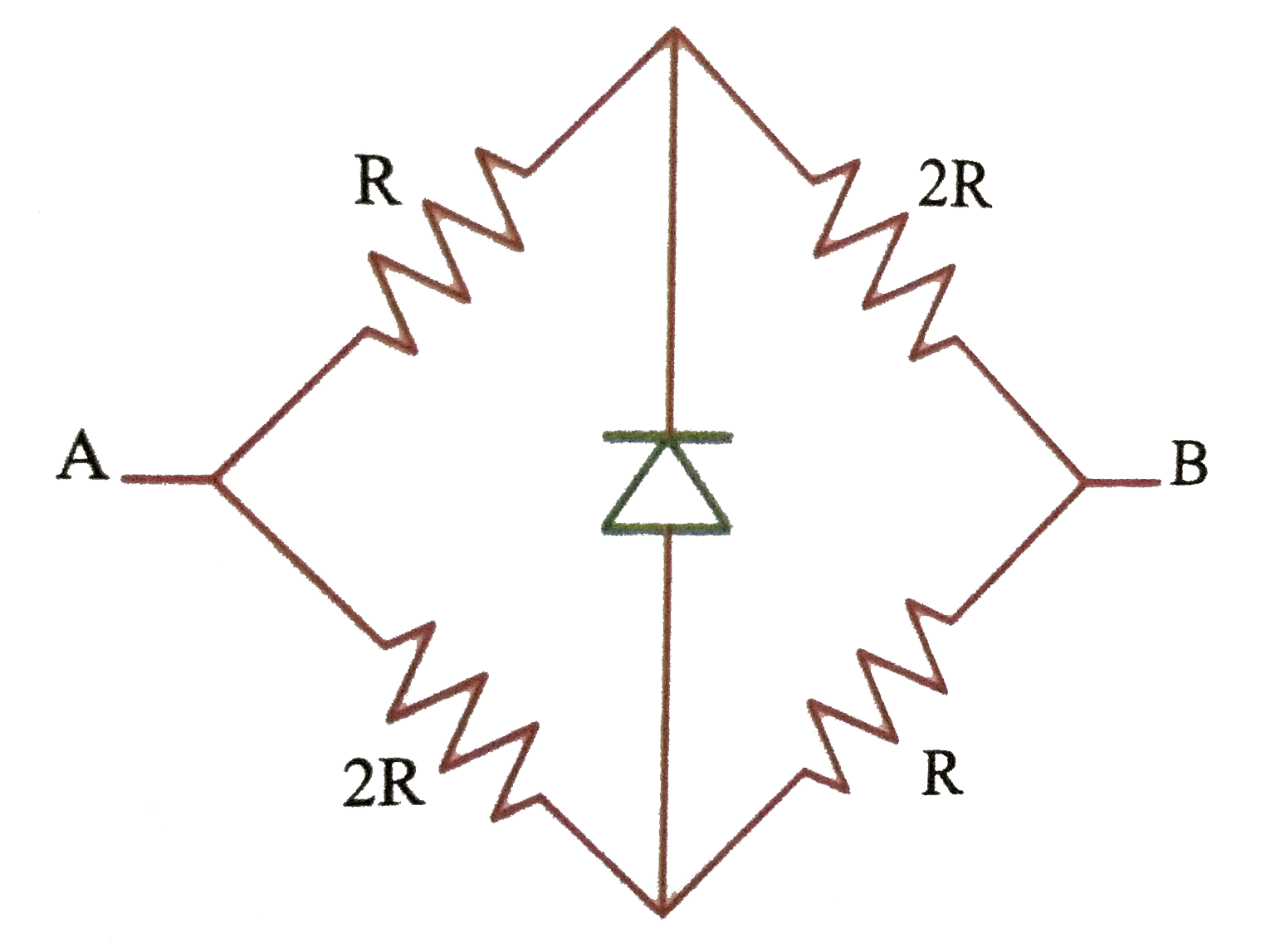 .
.
View SolutionThe equivalent resistance of the circuit across `AB` is given by
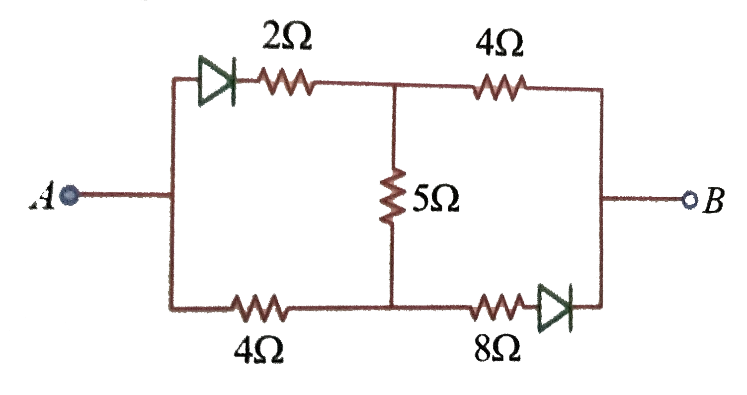 .
.
View SolutionThe equivalent resistance between `A` and `B` is
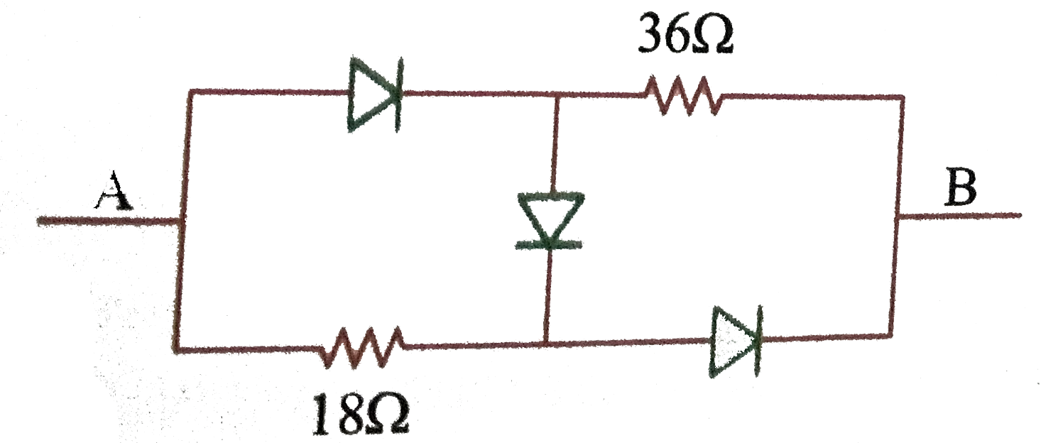 .
.
View SolutionA junction diode is connected to a `10 V` source and `10^(3) Omega` rheostat. The slope of load line on the characteristic curve of diode by `("in" A//V)`.
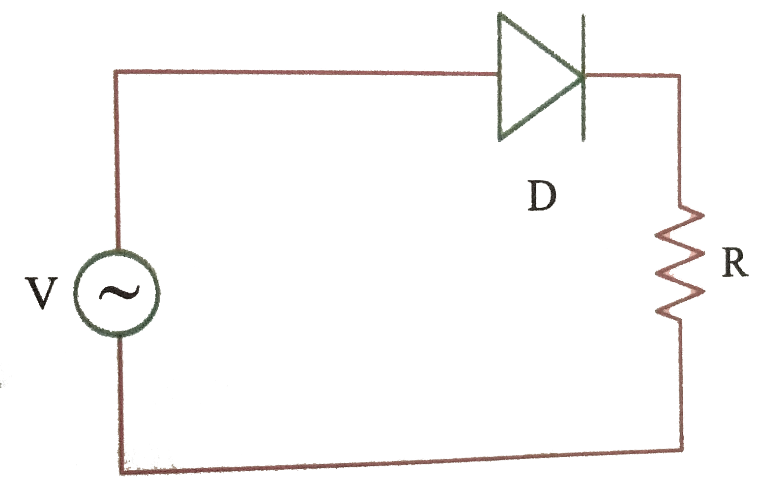
View SolutionA `p-n` junction `(D)` shown in the figure can act as a rectifier. An alternating current source `(V)` is connected in the circuit.
 .
.
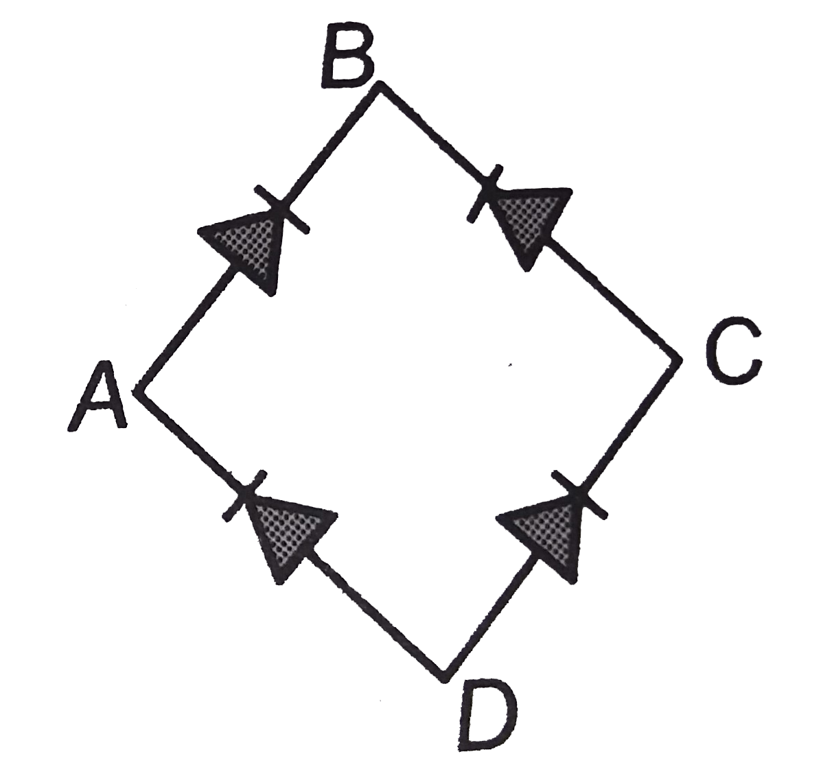
View SolutionIn the diagram, the input is across the terminals `A` and `C` and the output is across the terminals `B` and `D`, then the outputs is
View SolutionThe `I-V` characteristic of an `LED` is.
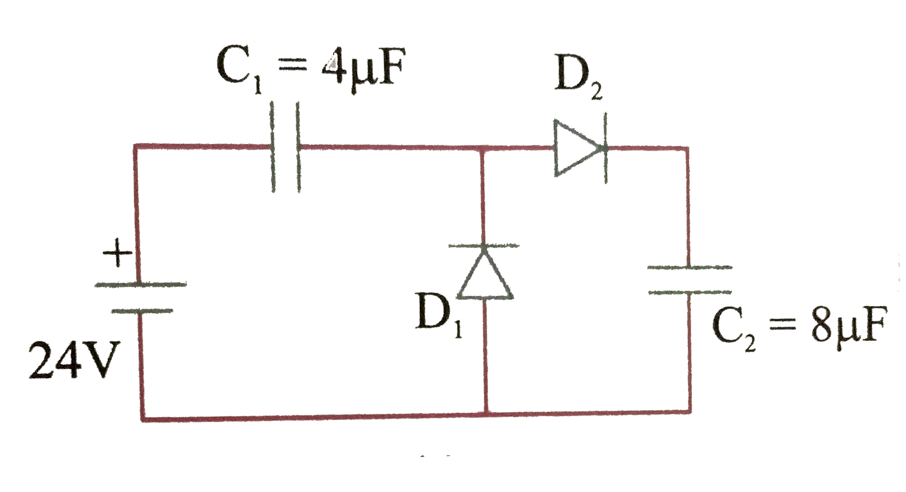
View SolutionIn the circuit shown. The potential drop across each capacitor is (assuming the two diodes are ideal).
 .
.
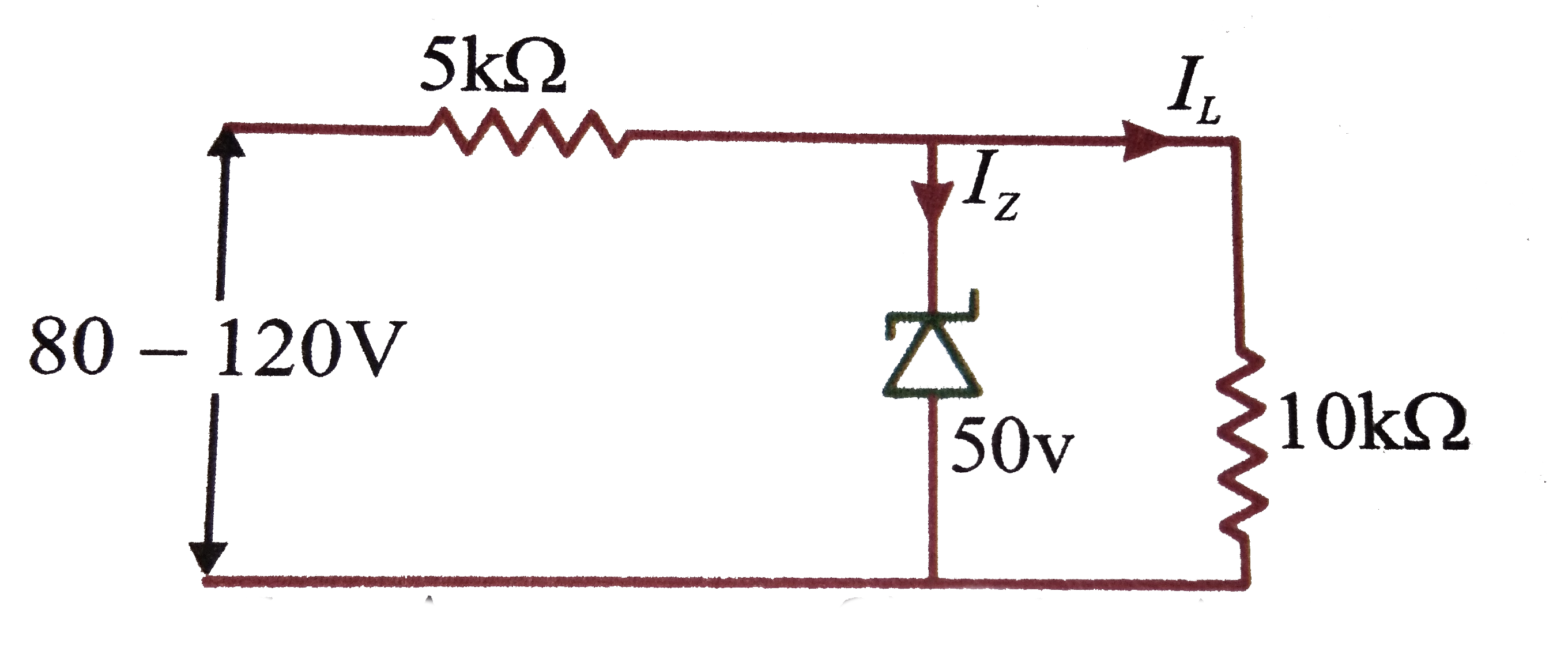
View SolutionThe maximum and minimum values of zener diode current are
View SolutionIn an n-p-n transistor circuit, the collector current ia 10 mA. If 90% of the electrons emitted reach the collector.
View SolutionThe constant `alpha` of a transistor is `0.9` What would be the change in the collector current corresponding to a change of `4mA` in the base current in a common emitter arrangement ?
View SolutionA voltage amplifier operated from a `12 `volt battery has a collector load `6 k Omega`. Calculate the maximum collector current in the circuit.
View SolutionIn a transistor circuit shown here the base current is `35 muA`. The value of the resistor `R_(b)` is
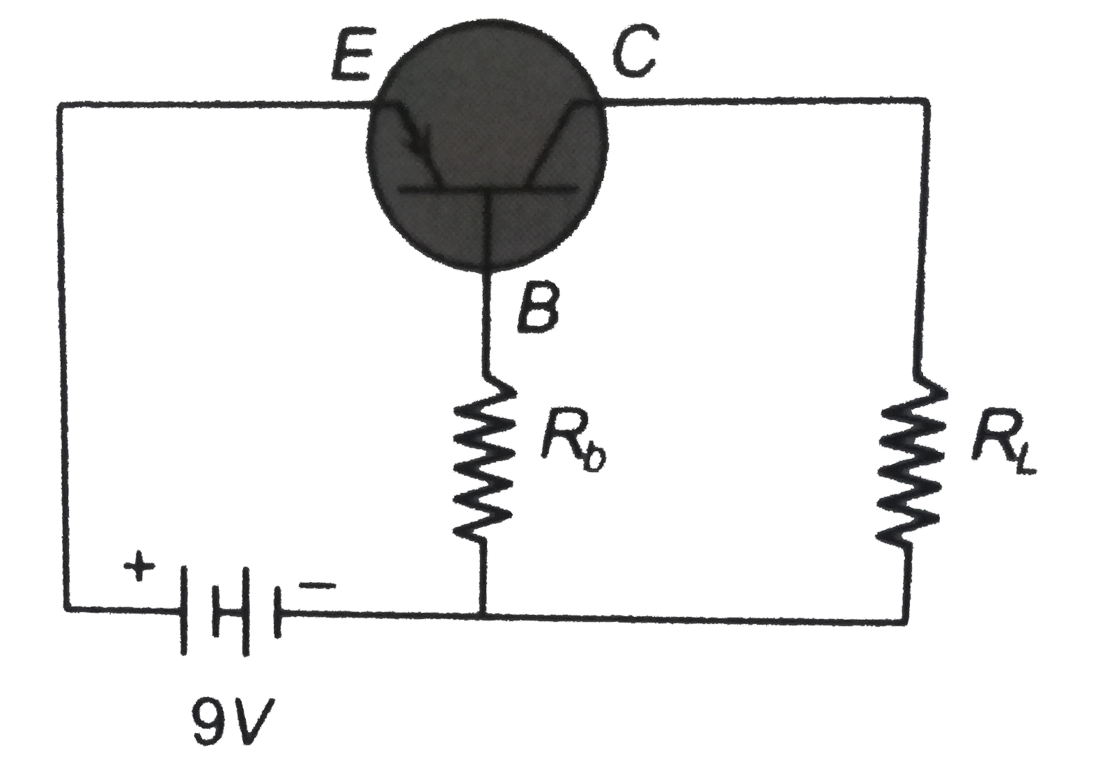
View SolutionIn a single state transistor amplifier, when the signal changes by `0.02 V` the base current by `10 mu A` and collector current by `1 mA`. If collector load `R_(C) = 2k Omega` and `R_(L) = 10 k Omega`, Calculate :
(i) Current Gain
(ii) Input Impedance,
(iii) Effective `AC` load,
(iv) Voltage gain and
(v) Power gain.
View SolutionOn subtracting `010101` from `101010`, we get :
View SolutionThe minimum number of gates required to realise this expression `Z = DABC + DA overline(BC)` is.
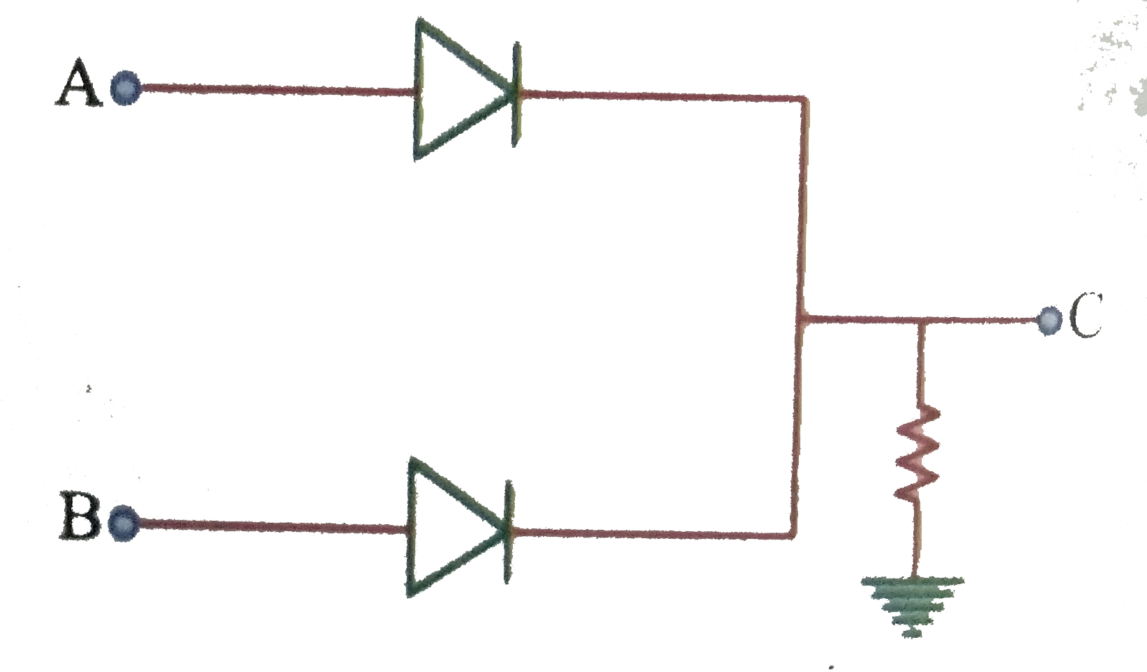
View SolutionIn the circuit below, `A` and `B` represents two inputs and `C` represents the output, the circuit represents.
 .
.
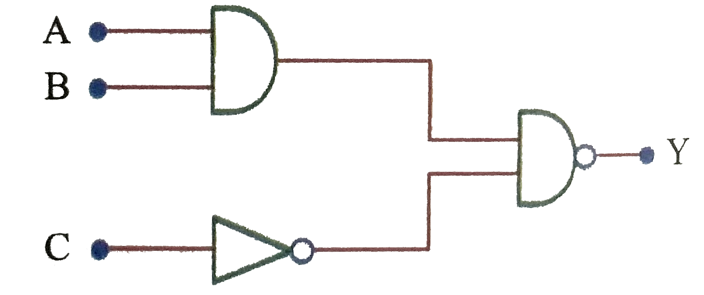
View SolutionIn the following circuit the output `Y` becomes zero for the inputs
 .
.
View SolutionThe combination of gates shown below yields
 .
.
View SolutionThe logic gate having an output of `1` is.
(i)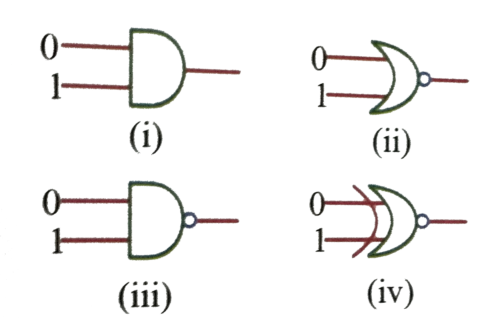
View SolutionIn a given circuit as shown the two input wave forms `A` and `B` are applied simultaneously.
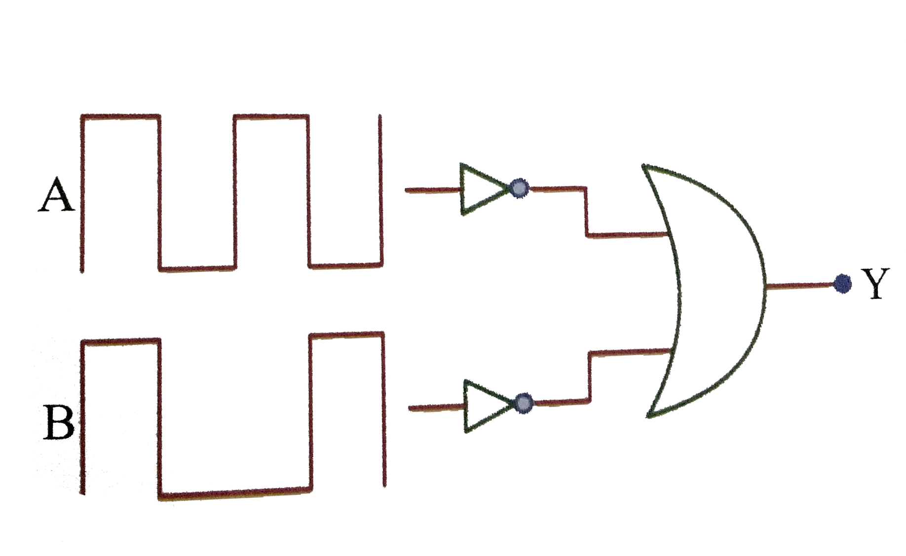
The resultant wave format at `Y` is.
View SolutionThe output of the combination of the gates shown in the figure below is
 .
.
View SolutionThe expression of `Y` in following circuit is
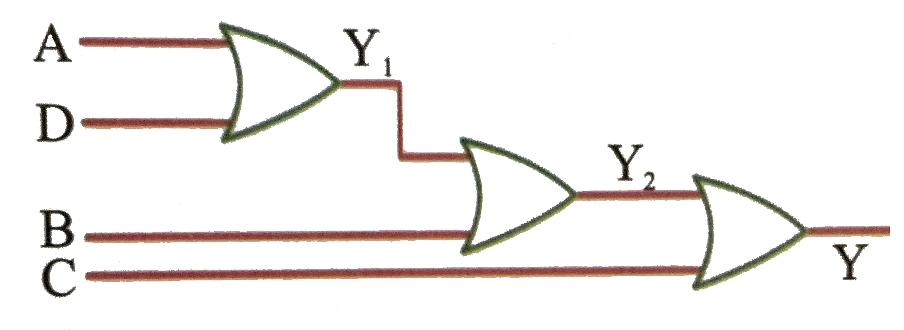 .
.
View SolutionHow many `NAND` gate are used to from `AND` gate?
View Solution
Level-II (C.W) questions and complete solutions for chapter SEMI CONDUCTOR DEVICES of NARAYANA PHYSICS (HINGLISH) of Class 12