Complete Solutions to ADDITIONAL EXERCISE (ASSERTION AND REASON TYPE QUESTIONS :) of chapter SEMICONDUCTOR ELECTRONICS of Class 12 book with complete answers and questions
| Class 12 | PHYSICS |
| Chapter | SEMICONDUCTOR ELECTRONICS |
| NARAYANA | ADDITIONAL EXERCISE (ASSERTION AND REASON TYPE QUESTIONS :) |
| Number Of Questions | 19 |
| Academic Year | 2023-24 |
Assertion : the following circuit represents 'OR' gate

Reason : for the above circuit `Y=barX=barbar (A+B)+A+B`
View SolutionAssertion : In the following circuit the potential drop across the resistance is zero.

Reason : The given resistance has low value.
View SolutionAssertion: `NOT` gate is also called inverter circuit.
Reason: `NOT` gate inverts the input order.
View SolutionAssertion: The current gain in common base circuit is always less than one.
Reason: At constant collector votalge the change in collector current is more than the change in emitter current.
View SolutionAssertion : The dominant mechanism for motion of charge carreis in forward and reverse biased silicon P-N junction are drit in both forward and reverse bias.
Reaon : In reverse biasing, no current flow through the junction.
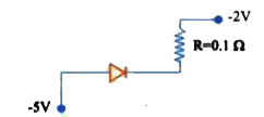
View SolutionAssertion : The value of current through p-n junction in the given figure will be 10 mA.

Reason : In the above figure, p-side is at higher potential than n-side.
View SolutionStatement-I : A p-n junction with reverse bias can be used as a photodiode to measure light intensity.
Statement-II : In a reverse bias condition the current in small but it is more sensitive to changes in incident light intensity.
View SolutionAssertion : In common base configuration, the current gain of the transistor is less than unity.
Reason : The collector terminal is revers biased for amplification.
View SolutionStatement-I : Germanium is preferred over silicon for making semiconductor devices
Statement-II : Energy gap for Ge is more than that of `SI`
View SolutionAssertion : The temparature coefficient of resistance is positive for metals and negative for semiconductors.
Reason : On raising the temperature in metals drift velocity increases but in semiconductors more change carries are released.
View SolutionAssertion : For a given applied voltage, conduction current in n-type semiconductor is more than in p-type semiconductors.
Reason : Mobility of electrons is greater than that of holes.
View SolutionAssertion : We cannot meausre that potential barrier of p-n junction by putting a sensitive voltmeter across its terminals.
Reason: In the depletion layer, there are no free elctrons or holes and in the absence of forward bias, it offers, infinite, resistance.
View SolutionAssertion : In Zener diode depletion layer is thin.
Reason : In reverse bias, strong electric field exists across the potential barrier.
View SolutionStatement-I : A p-n junction with reverse bias can be used as a photodiode to measure light intensity.
Statement-II : In a reverse bias condition the current in small but it is more sensitive to changes in incident light intensity.
View SolutionStatement-I : When base region has larger width, the collector current decreases.
Statement-II : In transistor, sum of base current and collector current is equal to emitter current.
View SolutionStatement-I : To be used as amplifier, the transistor in the common emitter confuration is preferred to the common base configuration.
Statement-II : In the common emitter, the signal is applied between emitter and base.
View SolutionAssertion : A transistor amplifier operates in active region.
Reason : In active region transistor characteristic is liner.
View SolutionAssertion: `NAND` or `NOR` gates are called digital building blocks.
Reason: The repeated use of `NAND` (or `NOR`) gates can produce all the basic or complicated gates.
View SolutionAssertion : In transistor, common emitter configuration is used to make a NOT gate.
Reason : In common emitter configuration, output voltage and input voltage have `180^(@)` phase difference.
View Solution
ADDITIONAL EXERCISE (ASSERTION AND REASON TYPE QUESTIONS :) questions and complete solutions for chapter SEMICONDUCTOR ELECTRONICS of NARAYANA PHYSICS (HINGLISH) of Class 12
All Exercises from NARAYANA Class 12 PHYSICS SEMICONDUCTOR ELECTRONICS
- ADDITIONAL EXERCISE (ASSERTION AND REASON TYPE QUESTIONS :)
- C.U.Q (APPLICATION OF JUNCTION DIODE AS RECTIFIER)
- C.U.Q (INTRINSIC AND EXTRINSIC SEMICONDUCTORS)
- C.U.Q (LOGIC GATES)
- C.U.Q (SPECIAL PURPOSE P-N JUNCTION DIODES)
- EVALUATE YOURSELF-1
- EVALUATE YOURSELF-2
- EVALUATE YOURSELF-3
- EVALUATE YOURSELF-4
- EXERCISE -1 (C.W) (APPLICATION OF JUNCTION DIODE AS RECTIFIER)
- EXERCISE -1 (C.W) (INTRINSIC AND EXTRINSIC SEMICONDUCTORS)
- EXERCISE -1 (C.W) (JUNCTION DIODE)
- EXERCISE -1 (C.W) (LOGIC GATES)
- EXERCISE -1 (C.W) (TRANSISTORS)
- EXERCISE -1 (H.W) (APPLICATION OF JUNCTION DIODE AS RECTIFIER
- EXERCISE -1 (H.W) (INTRINSIC AND EXTRINSIC SEMICONDUCTORS)
- EXERCISE -1 (H.W) (JUNCTION DIODE)
- EXERCISE -1 (H.W) (LOGIC GATES)
- EXERCISE -1 (H.W) (TRANSISTORS)
- EXERCISE -2 (C.W) (APPLICATIONS OF JUNCTION DIODE AS RECTIFIER)
- EXERCISE -2 (C.W) (JUNCTION DIODES)
- EXERCISE -2 (C.W) (LOGIC GATES)
- EXERCISE -2 (C.W) (TRANSISTORS)
- EXERCISE -2 (C.W) INTRINSIC, EXTRINSIC SEMICONDUCTONS)
- EXERCISE -2 (H.W) (APPLICATIONS OF JUNCTION DIODE AS RECTIFIER)
- EXERCISE -2 (H.W) (INTRINSIC, EXTRINSIC SEMICONDUCTORS)
- EXERCISE -2 (H.W) (JUNCTION DIODES)
- EXERCISE -2 (H.W) (LOGIC GATE)
- EXERCISE -2 (H.W) (TRANSISTORS)
- EXERCISE -3
- EXERCISE-4
- ILLUSTRATION