Complete Solutions to ILLUSTRATION of chapter SEMICONDUCTOR ELECTRONICS of Class 12 book with complete answers and questions
| Class 12 | PHYSICS |
| Chapter | SEMICONDUCTOR ELECTRONICS |
| NARAYANA | ILLUSTRATION |
| Number Of Questions | 30 |
| Academic Year | 2023-24 |
The energy gap of germanium is 1.28 eV. What is the maximum wave length at which germanium will begin absorbing energy.
View SolutionPure Si at 400K has equal electron `(n_(e))` and hole `(n_(h))` concentrations of `3xx10^(16)m^(-3)`. Doping by indium, `n_(h)` increases to `6xx10^(22)m^(-3)`. Calculate `n_(e)` in the doped Si.
View SolutionSuppose a pure Si crystal has `6xx10^(28)` atoms `m^(-3)`. It is doped by 1ppm concentration of pentavalent As. Calculate the number of electrons and holes, Given that `n_(i)=0.5xx10^(16)m^(-3)`
View SolutionWhy Carbon acts as insulator while Silicon and Germanium act as semiconductors?
View SolutionFind voltage across resistor, and current through diode.

View SolutionIf each diode forward resistance is `50omega` then find current through the `100omega` resistor in the given circuit.

View SolutionIs reverse saturation current of a diode independent of reverse bias voltage?
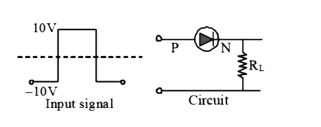
View SolutionIf the following input signal is sent through a P-N junction diode, then the output signal across `R_L` will be -
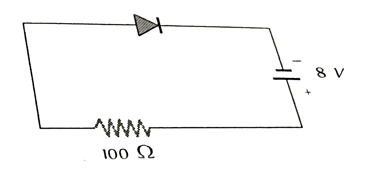
View SolutionA source voltage of 8 V drives the diode in fig. through a current- limiting resistor of 100 ohm . Then the magnitude of the slope load line on the V - I characteristics of the diode is
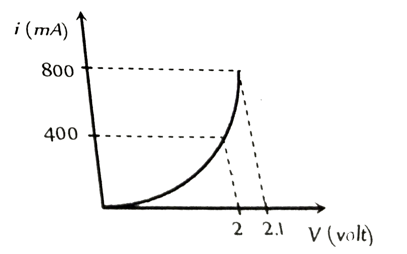
View SolutionThe i - V characteristic of a P - N junction diode is shown below. The approximate dynamic resistance of the P - N junction when a forward bias of 2 volt is applied
View SolutionIn half wave rectifier a p-n diode with internal resistance `20Omega` is used. If the load resistance of `2kOmega` is used in the circuit, then find the efficiency of this half wave rectifier.
View SolutionIn the half-wave rectifier circuit shown, which one of the following waveform is true for `V_(CD)` the output across C and D?

View SolutionIn a zener regulated power supply, a zener diode with `V_(Z)=5.0V` is used for regurlation. The load current is to be 2.0 mA and the unregulated input is 10.0V. What should be the value of series resistance `R_(S)`?
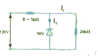
View SolutionFrom the zener diode circuit shown in the figure, find (1) the output voltage (2) the voltage drop across series resistance and (3) the current through zener diode.
View SolutionThe current in the forward bias is unknown to be more (~mA) than the current in the reverse bias (`~muA`). What is the reason then to operate the photo diodes in reverse bias ?
View SolutionWhy are Si and GaAs are preferred materials for solar cells?
View SolutionThe base current is `100 muA` and collector current is 3 mA
(a) Calculate the values of `beta,I_(e)` and `alpha`
(b) A change of `20 muA` in the base current produces a charge of 0.5 mA in the collector current. Calculate `beta_(ac)`
View SolutionFor a CE transistor amplifier, the audio signal voltage across the collector resistance of `4.0kOmega` is 4.0V. suppose the current amplification factor of the transistor is 100. What should be the value of `R_(B)` in series with supply of 2.0 V if the de base current has to be 10 times the signal current. Also calculate the dc drop across the `V_(BB)` collector resistance.
View SolutionIn a transistor, the value of `beta` is 60 Calculate the value of `alpha` .
View SolutionWhy the emitter is forward biased and the collector is reverse biased in a transistor?
View SolutionIn a transistor, connected in common emitter mode `R_(0)=5kOmega," "R_(i)=1kOmega," "I_(C)=1mA,I_(B)=40muA`. Find the voltage gain.
View SolutionExplain why a transistor is preferred in CE configuration over the CB configuration?
View SolutionIn a negative feedback amplifier, the gain without feedback in `100`, feed back ratio is `1//25` and input voltage is `50 m V`. Calculate
(i) gain with feedback
(ii) feedback factor
(iii) output voltage
(iv) feedback voltage
(v) new input voltage so that output voltage with feedback equals the output voltage without feedback.
View SolutionThe Boolean expression of the output `Y` of the inputs `A` and `B` for the circuit shown in the fig.
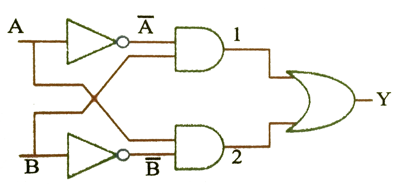 .
.
View SolutionThe diagram of a logic circuit is given below. The output of the circuit is reprsented by

View SolutionThe logic circuit and its truth table are given, what is the gate `X` in the diagram
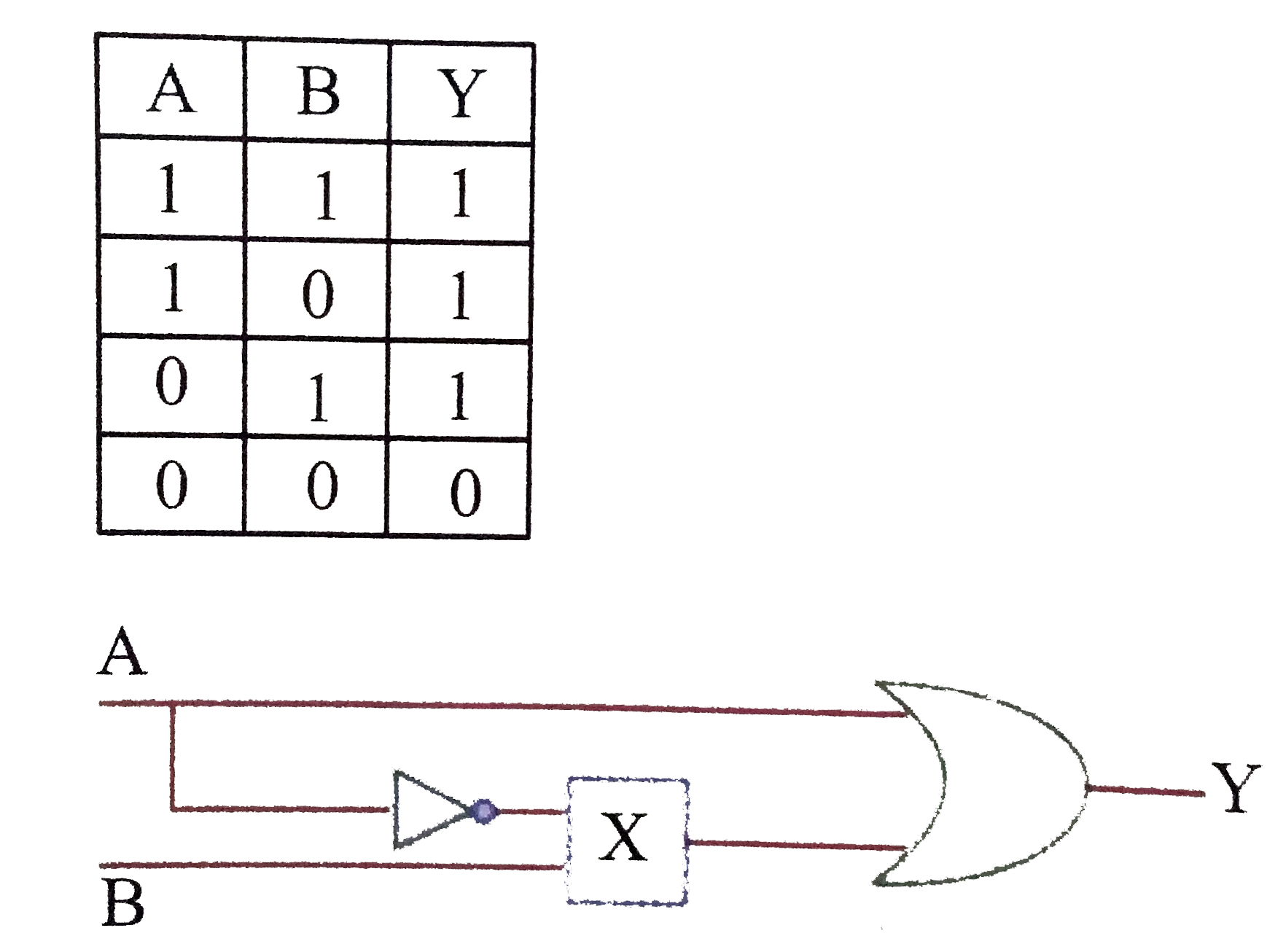 .
.
View SolutionYou are given two circuit as shown in Fig.and . Which consists of NAND gates. Identify the logic operation carried out by the two circuits.

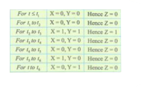
View SolutionTake X and Y input waveforms. Sketch the output (Z) waveform abtained from AND gate as per the following conditions:
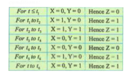
View SolutionSketch the output Y from a OR gate having inputs X and Y as per the following conditions:
View SolutionWhich represents NAND gate?
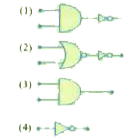
View Solution
ILLUSTRATION questions and complete solutions for chapter SEMICONDUCTOR ELECTRONICS of NARAYANA PHYSICS (HINGLISH) of Class 12
All Exercises from NARAYANA Class 12 PHYSICS SEMICONDUCTOR ELECTRONICS
- ADDITIONAL EXERCISE (ASSERTION AND REASON TYPE QUESTIONS :)
- C.U.Q (APPLICATION OF JUNCTION DIODE AS RECTIFIER)
- C.U.Q (INTRINSIC AND EXTRINSIC SEMICONDUCTORS)
- C.U.Q (LOGIC GATES)
- C.U.Q (SPECIAL PURPOSE P-N JUNCTION DIODES)
- EVALUATE YOURSELF-1
- EVALUATE YOURSELF-2
- EVALUATE YOURSELF-3
- EVALUATE YOURSELF-4
- EXERCISE -1 (C.W) (APPLICATION OF JUNCTION DIODE AS RECTIFIER)
- EXERCISE -1 (C.W) (INTRINSIC AND EXTRINSIC SEMICONDUCTORS)
- EXERCISE -1 (C.W) (JUNCTION DIODE)
- EXERCISE -1 (C.W) (LOGIC GATES)
- EXERCISE -1 (C.W) (TRANSISTORS)
- EXERCISE -1 (H.W) (APPLICATION OF JUNCTION DIODE AS RECTIFIER
- EXERCISE -1 (H.W) (INTRINSIC AND EXTRINSIC SEMICONDUCTORS)
- EXERCISE -1 (H.W) (JUNCTION DIODE)
- EXERCISE -1 (H.W) (LOGIC GATES)
- EXERCISE -1 (H.W) (TRANSISTORS)
- EXERCISE -2 (C.W) (APPLICATIONS OF JUNCTION DIODE AS RECTIFIER)
- EXERCISE -2 (C.W) (JUNCTION DIODES)
- EXERCISE -2 (C.W) (LOGIC GATES)
- EXERCISE -2 (C.W) (TRANSISTORS)
- EXERCISE -2 (C.W) INTRINSIC, EXTRINSIC SEMICONDUCTONS)
- EXERCISE -2 (H.W) (APPLICATIONS OF JUNCTION DIODE AS RECTIFIER)
- EXERCISE -2 (H.W) (INTRINSIC, EXTRINSIC SEMICONDUCTORS)
- EXERCISE -2 (H.W) (JUNCTION DIODES)
- EXERCISE -2 (H.W) (LOGIC GATE)
- EXERCISE -2 (H.W) (TRANSISTORS)
- EXERCISE -3
- EXERCISE-4
- ILLUSTRATION