Complete Solutions to Exercise of chapter SOLID AND SEMICONDUCTOR DEVICES of Class 12 book with complete answers and questions
| Class 12 | PHYSICS |
| Chapter | SOLID AND SEMICONDUCTOR DEVICES |
| NEET PREVIOUS YEAR | Exercise |
| Number Of Questions | 100 |
| Academic Year | 2023-24 |
The given electrical network is equivalent to:

View SolutionIn a common emitter transistor transistor amplifier, the audio signal voltage across the collector is `3kOmega`. If current gain is 100 and the base resistance is `2kOmega`, the voltage and power gain of the amplifier are
View SolutionWhich one of the following represents forward bias diode?
View SolutionTo get output `1`for the following circuit, the correct choice for the input is :

View SolutionConsider the junction diode as ideal. The value of current flowing throgh `AB` is:

View SolutionA `"n-p-n"` transisitor is connected in common emitter configuration in a given amplifier. A load resistance of `800 Omega` is connected in the collector circuit and the voltage drop across it is `0.8 V`. If the current amplification factor is `0.96` and the input resistance of the circuits is `192 Omega`, the voltage gain and the power gain of the amplifier will respectively be
View SolutionFor CE transistor amplifier, the audio signal voltage across the collector resistance of `2 kOmega` is 4V. If the current amplification factor of the transistor is 100 and the base resistance is `1kOmega`, then the input signal voltage is
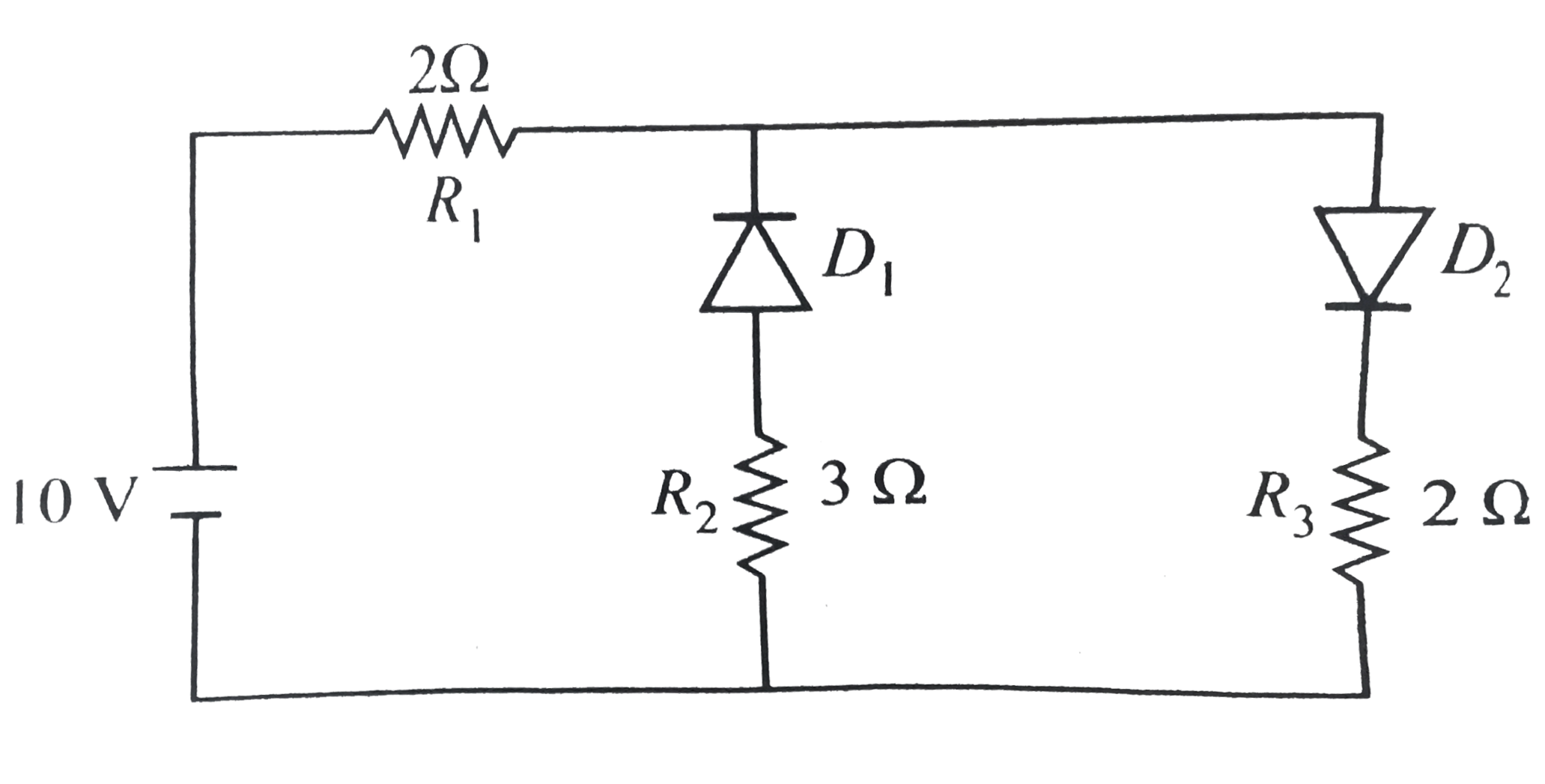
View SolutionThe given circuit has two ideal diodes connected as show in the figure. The current flowing through the resistance `R_(1)` will be
View SolutionWhat is the output `Y` in the following circuit, when all the three output `A,B,C` are first `0` and then `1`?

View SolutionIf a `p-n` junction diode, a square input signal of `10 V` is applied as shown.
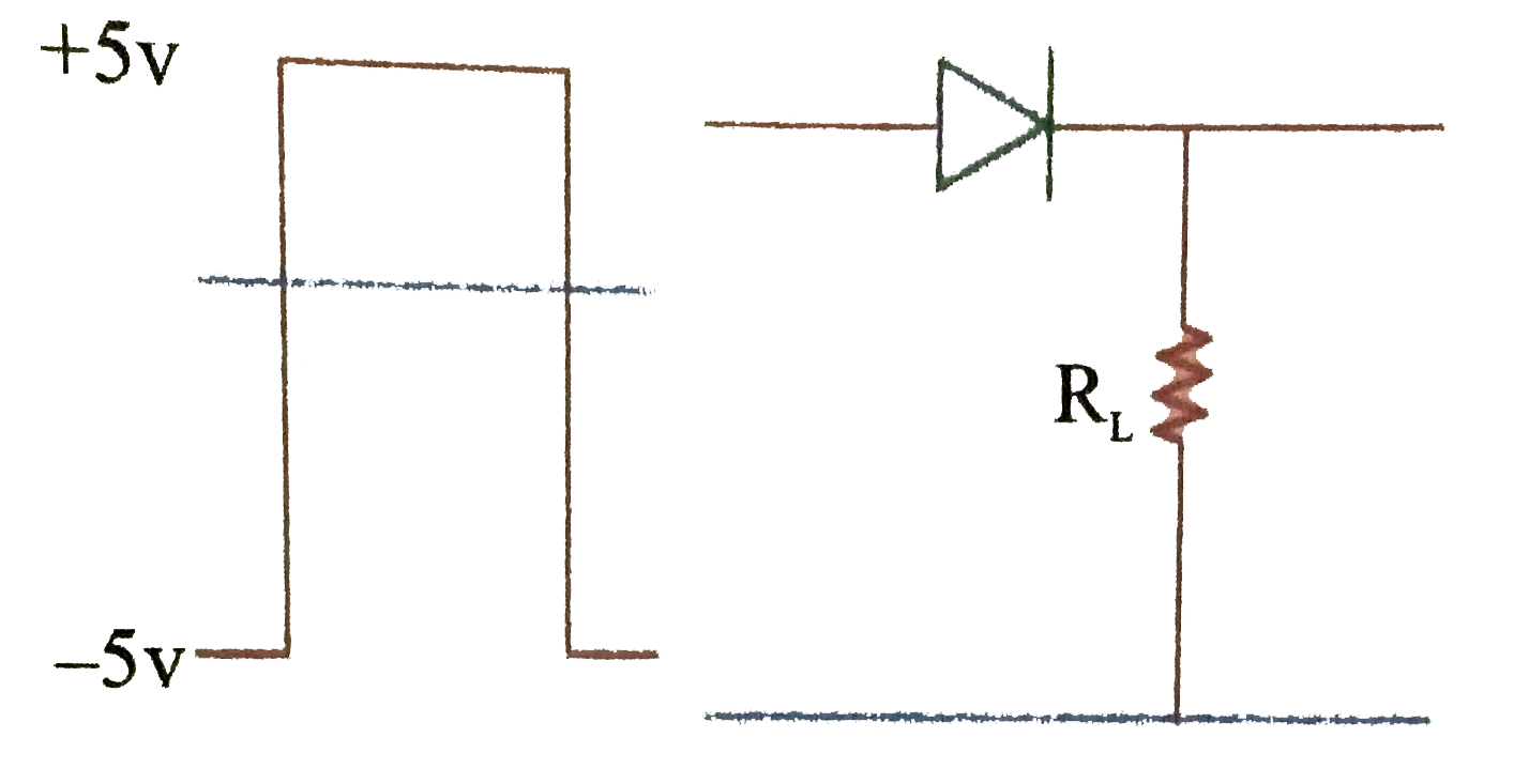
Then the out put signal across `R_(L)` will be
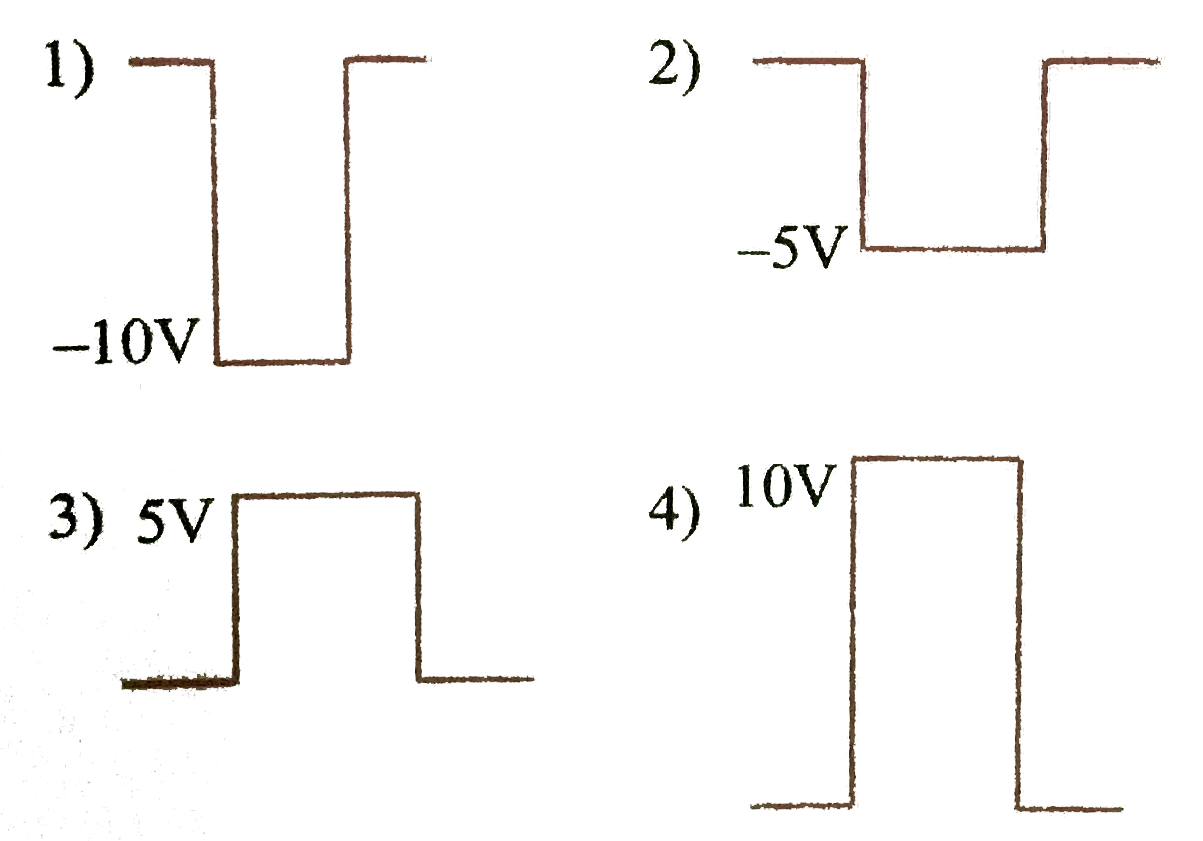 .
.
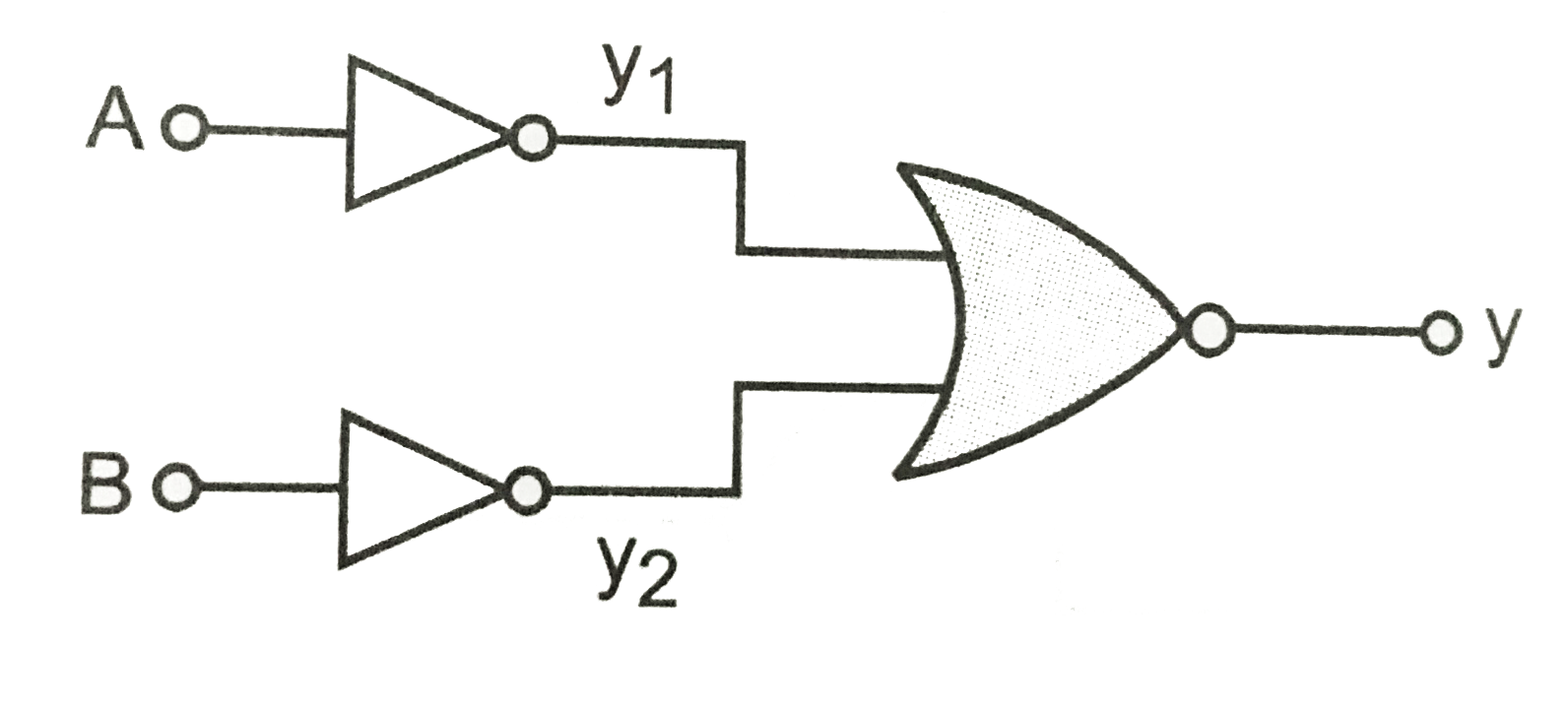
View SolutionWhich logic gate is represented by the following combination of logic gates
View SolutionThe input signal given to a `CE` amplifier having a voltage gain of `150` is `V_(i)=2cos(15t+(pi)/3)`. The corresponding output signal will be
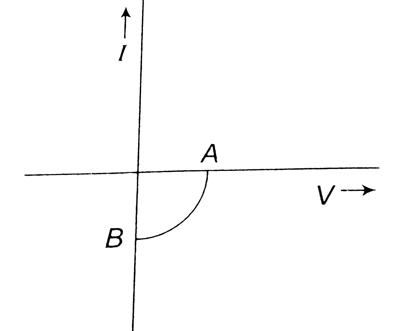
View SolutionThe given graph represents `V-I` characteristic for a semiconductor device.
which of the following statement is correct?
View SolutionThe barrier potential of a p-n junction depends on : (i) type of semiconductor material (ii) amount of doping (iii) temperature.
Which is one of the following is correct?
View SolutionIn a `n`-type semiconductor, which of the following statement is true?
View SolutionIn a common emitter (CE) amplifier having a voltage gain G, the transistor used has transconductor 0.03 `mho` and current gain 25. If the above transistor is replaced with another one with transconductance 0.02 `mho` and current gain 20, the voltage gain will
View SolutionThe output `(X)` of the logic circuit shown in figure will be

View SolutionIn a CE transistor amplifier, the audio signal voltage across the collector resistance of `2kOmega` is `2V`. If the base resistance is `1kOmega` and the current amplification of the transistor is 100, the input signal voltage is:
View Solution`C` and `Si` both have same lattice structure, having `4` bonding electrons in each. However, `C` is insulator whereas `Si` is intrinsic semiconductor. This is because
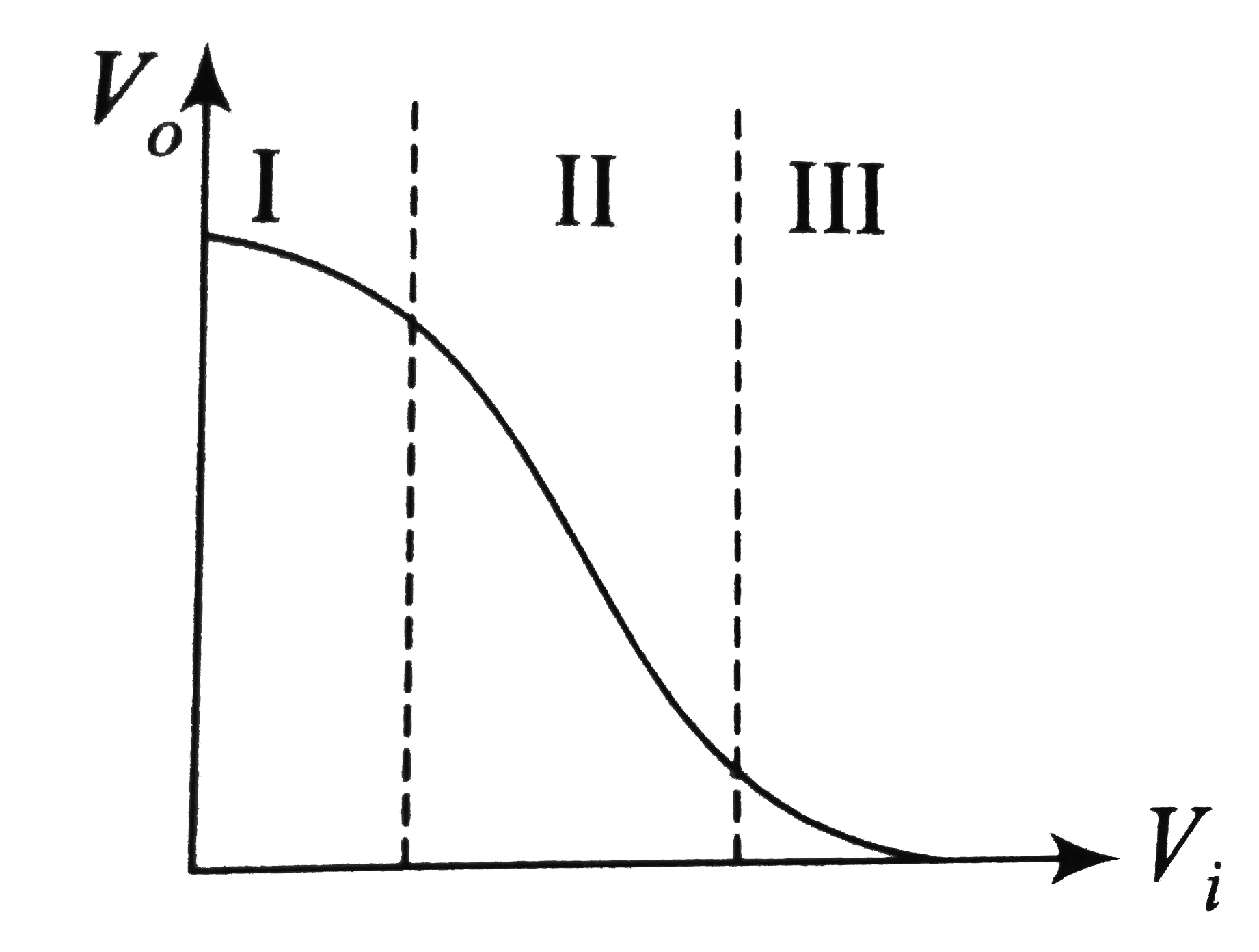
View SolutionTransfer characterstics [output voltage `(V_(o))` vs. input voltage `(V_(i))`] for a base biased transistor in `CE` configuration is as shown in the figure. For using transfor as a which, it is used
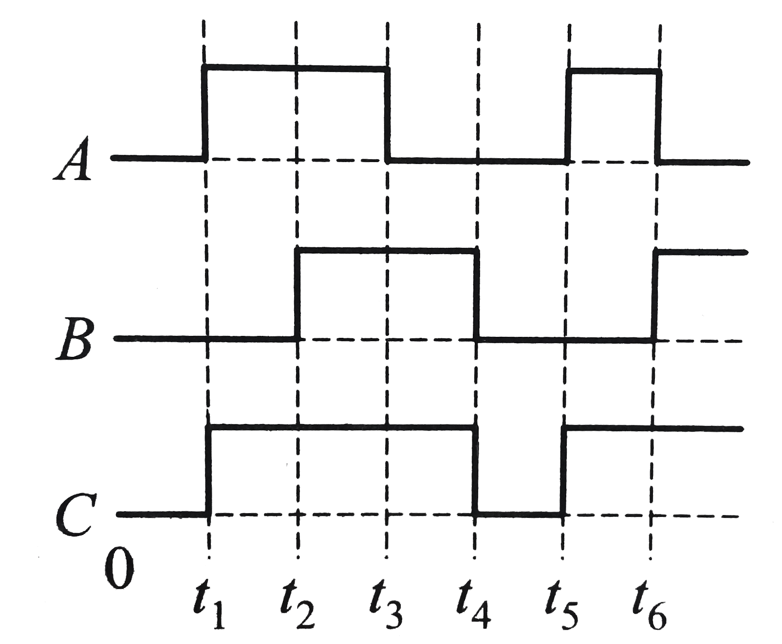
View SolutionThe figure shows a logic circuit with two inputs `A` and `B` and the output `C`. The voltage wave forms across `A,B` and `C` are as given. The logic circuit gate is
View SolutionSymbolic representation of four logic gates are shown as
(i)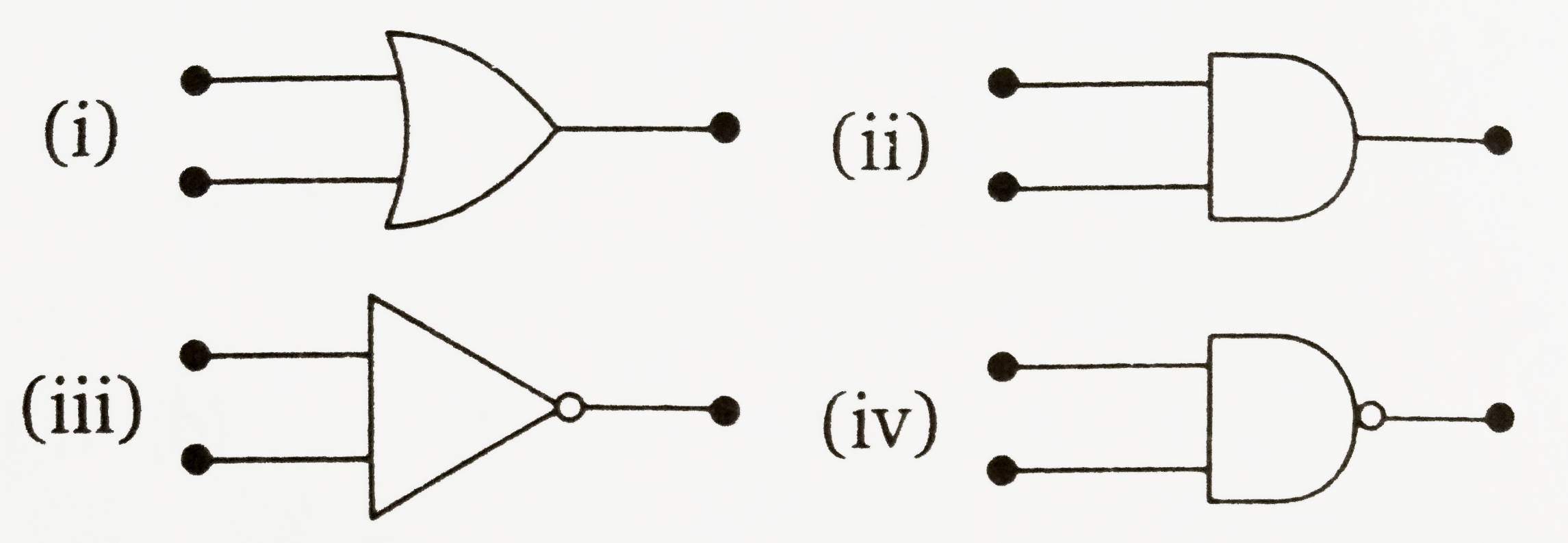
Pick out which ones are for AND, NAND and NOT gates, respectively.
View SolutionIf a small amount of antimony is added to germanium crystal
View SolutionIn forward biasing of the p-n junction:
View SolutionWhich one of the following statement is false?
View SolutionThe device that can act as a complete electronic circuit is
View SolutionA common emitter amplifier has a voltage gain of `50`, an input impedence of `100 Omega` and an output impedence of `200 Omega`. The power gain of the of the amplifier is
View SolutionTo get an output `y=1` from the circuit shown below, the input must be

View SolutionSodium has body centred packing. Distance between two nearest atoms is `3.7 Å`. The lattice parameter is
View SolutionA transistor is operated in common emitter configuration at `V_(c)=2 V` such that a change in the base current from `100 muA` to `200 muA` produces a change in the collector current from `5 mA` to `10 mA`. The current gain is
View SolutionThe symbolic representation of four logic gates are given in Fig.The logic symbol for OR, NOT and NAND gates are respectively

View SolutionA `p-n` photodiode is fabricated from a semiconductor with a band gap of `2.5 eV`. It can detect a signal of wavelength
View SolutionThe circuit is equivalent to

View SolutionA `p-n` photodiode is made of a material with a band gap of `2.0 eV`. The minimum frequency of the radiation that can be absorbed by the material is nearly
View SolutionThe voltage gain of an amplifier with `9%` negative feedback is `10`. The voltage gain without feedback will be
View SolutionIf the lattice parameter for a crystalline structure is `3.6Å`, then the atomic radius is fcc crystals is
View SolutionFor a cubic crystal structure which one of the following relations indicating the cell characterstic is correct?
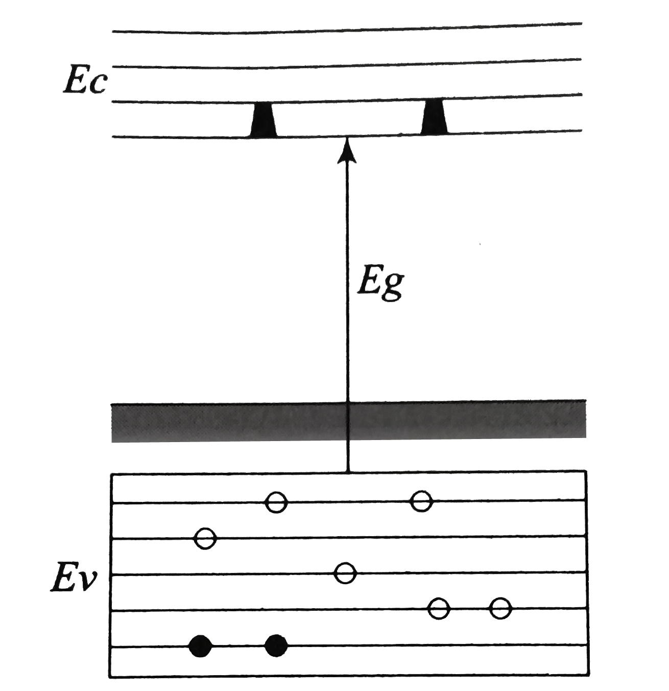
View SolutionIn the energy band diagram of a material shown below, the open circles and filled circles denote holes and electrons respectively. The material is a/an
View SolutionIn the following circuit, the output `Y` for all possible inputs `A` and `B` is expressed by the truth table:

View SolutionThe following figure shows a logic gate circuit with two inputs A and B output C. The voltage waveforms of A,B and C are as shown in second figure given below :-
_E01_436_Q01.png)
The logic circuit gate is :-
View SolutionA forward biased diode is
View SolutionA transistor is operated in common emitter configuration at constant collector voltage `V_(c)=1.5 V` such that a change in the base current from `100 muA` to `150 muA` produces a change in the collector current from `5 mA` to `10 mA`. The current gain `(beta)` is
View SolutionA transistor -oscillator using a resonant circuit with an inductor `L` (of negligible resistance) and a capacitor `C` in series produce oscillations of frequency `f`. If `L` is doubled and `C` is changed to `4C`, the frequency will be
View SolutionCopper has face centred cubic `(fc c)` lattice with interatomic spacing equal to `2.54 Å`. The value of the lattice constant for this lattice is
View SolutionChoose the only false statement form the following
View SolutionCarbon , silicon and germanium have four valence elcectrons each . These are characterised by valence and conduction bands separated by energy band - gap respectively equal to ` (E_g)_(c) (E_g)_(si) ` and ` (E_g)_(Ge) `. Which of the following statements ture ?
View SolutionZener diode is used for
View SolutionApplication of a forward biase to a `"p-n"` junction:
View SolutionOf the diodes shown in the following diagrams, which one is reverse biased?
View SolutionIn a `"p-n"` junction photo cell, the value of the photo electromotive force produced by monochromatic light is proportional to
View SolutionThe output of `OR` gate is `1`
View SolutionThe peak voltage in the output of a half-wave diode rectifier fed with a sinusiodal signal without filter is `10 V`. The `dc` component of the output voltage is
View SolutionIn semiconductors at a room tempreture
View SolutionA `npn` transistor conducts when
View SolutionIf a full wave reactifier circuit is operating from `50 Hz` mains, the fundamental frequency in the ripple will be
View SolutionBarrier potential of a `"p-n"` junction diode does not depend on
View SolutionFollowing diagram performs the logic function of

View SolutionFor the given circuit of `PN`-junction diode, which of the following statements is correct?
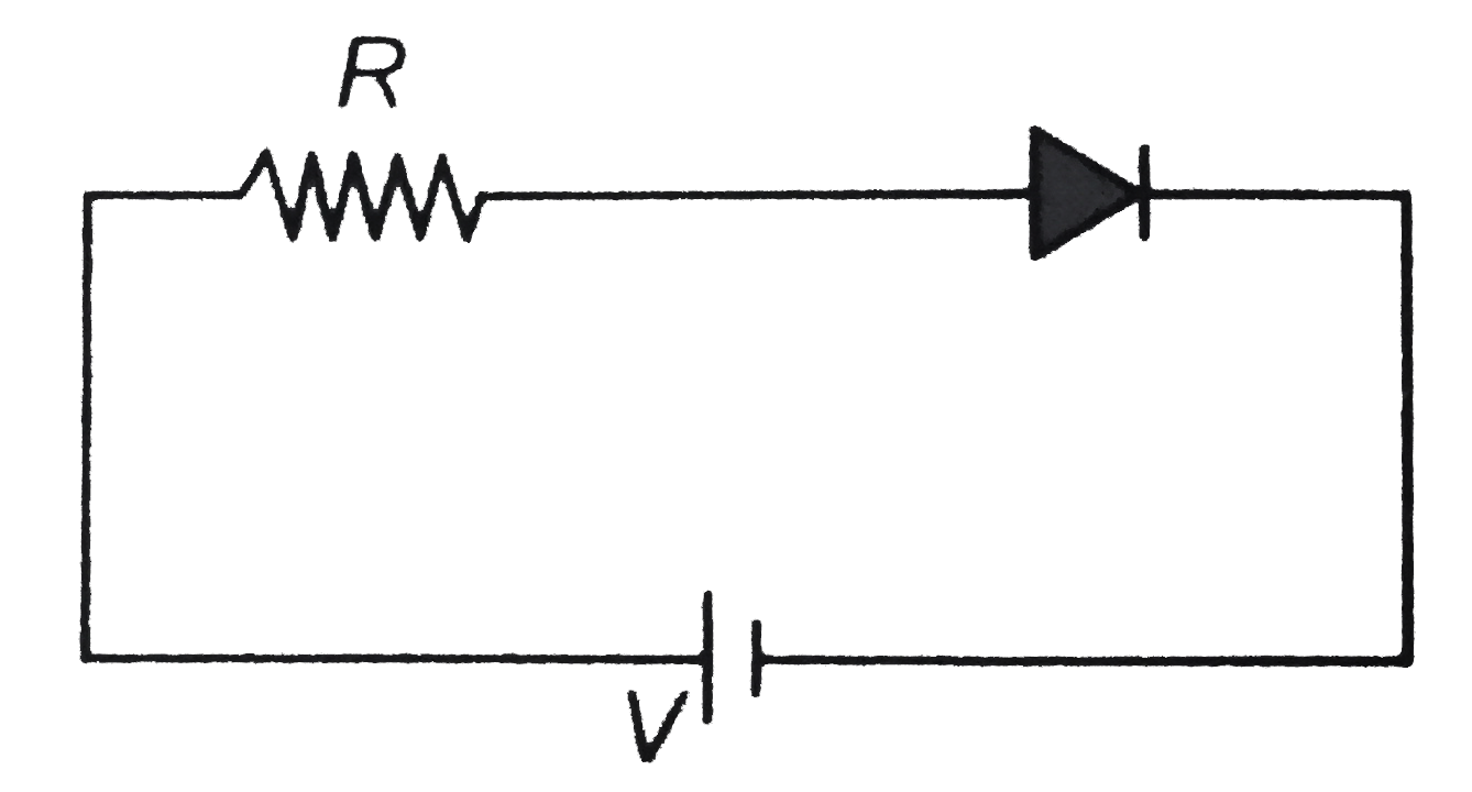
View SolutionFor conduction in a `"p-n"` junction, the biasing is
View SolutionFor a transistor `(I_(C))/(I_(E))=0.96`, then current gain for common emitter configuration
View SolutionThe number of atoms per unit cell in bcc lattice is
View SolutionIn bcc structure of lattice constant a, the minimum distance between atoms is
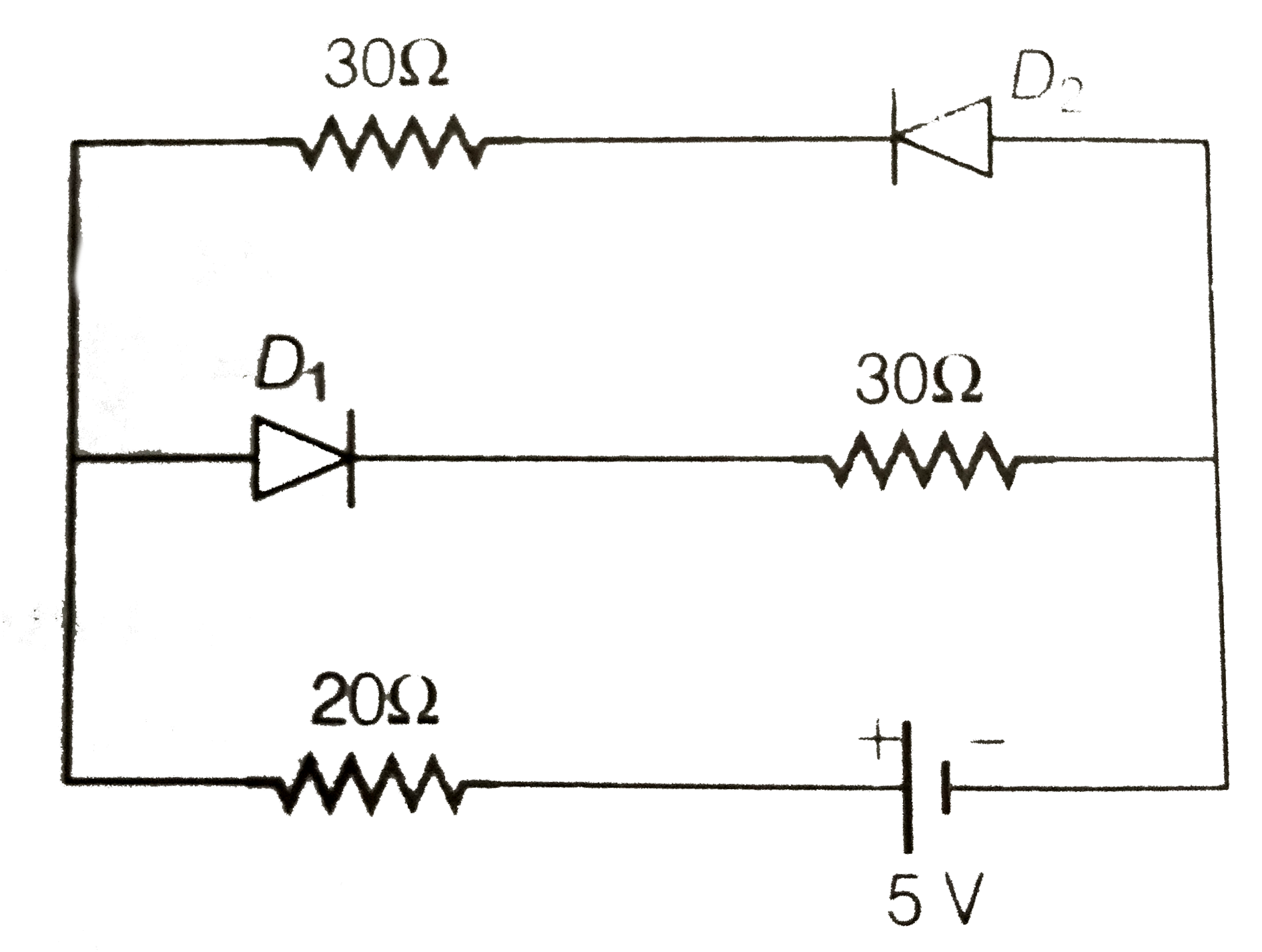
View SolutionIf internal resistance of cell is negligible, then current flowing through the circuit is
View SolutionIn a common-base configuration of a transistor `(Delta i)/(Delta i_(e)) = 0.98`, then current gain in common emitter configuration of transistor will be
View SolutionSi and Cu are cooled to a temperature of `300 K`, then resistivity
View SolutionIn which of the following figures, junction diode is forward biased?
View SolutionThe truth table given below represents

View SolutionIf `alpha` and `beta` current gains in common-base and common-emitter configuration of a transistor, then `beta` is equal to
View Solution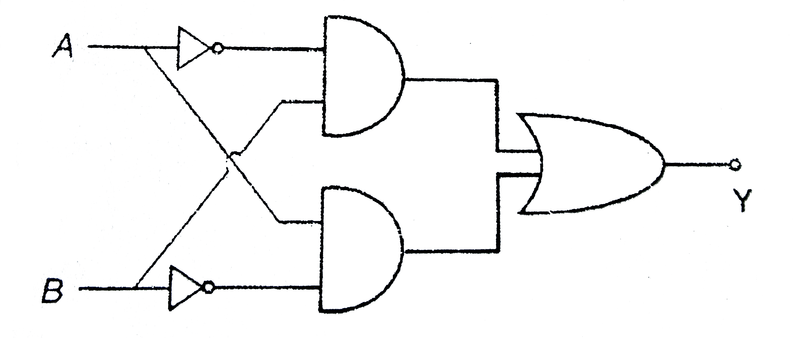
The following circuit represents:
View SolutionIn `P`-type semiconductor the majority and minorty charge carriers are respectively
View SolutionIn forward bias, the width of potential barrier in a `P-N` junction diode
View SolutionDepletion layer consists of
View SolutionIn junction diode, the holes are due to
View SolutionWhich of the following when added as an impurity into silicon produces n-type semicondutor ?
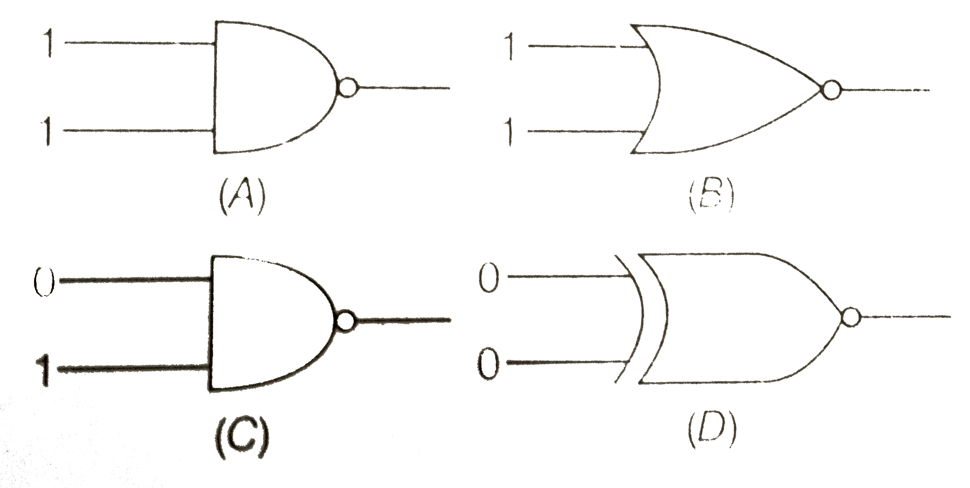
View SolutionWhich one of the following gates will have an output of 1 ?
View SolutionThe transfer ration of a transistor is `50`. The input resistance of the transistor when used in the common -emitter configuration is `1 kOmega`. The peak value for an `A.C.` input voltage of `0.01 V` peak is
View SolutionA semiconducting device is connected in a series circuit with a battery and a resistance.A current is found to pass through the circuit .If the polarity of the battery is reversed, the current drops to almost zero.The device may be
View SolutionThe cause of the potential barrier in a p-n diode is:
View SolutionThe following truth table belongs to which of the following four gates ?

View SolutionThe relation between `alpha` and `beta` parameters of current gains for a transistors is given by
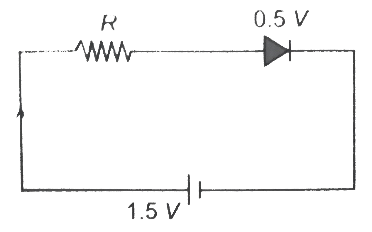
View SolutionThe diode used in the circuit shown in the figure has a constant voltage drop of `0.5 V` at all currents and a maximum power rating fo `100` milliwatts. What should be the value of the resistor `R`, connected in series with the diode for obtaining maximum current?
View SolutionTo obtain a `P`-type germanium semiconductor, it must be dopped with
View SolutionWhen arsenic is added as an impurity to silicon, the resulting material is
View SolutionThe current gain for a transistor working as a common-base amplifier is `0.96`. If the emitter current is `7.2 mA`, the base current will be
View SolutionWhen N-P-N transistor is used as an amplifier-
View SolutionWhich of the following , when added as an impurity, into the silicon, produces n-type semiconductor ?
View SolutionWhich of the following gates corresponds to the truth table given below ?

View SolutionIn the figure, the input is across the terminals
A and C and the output is across B and D. Then the output is
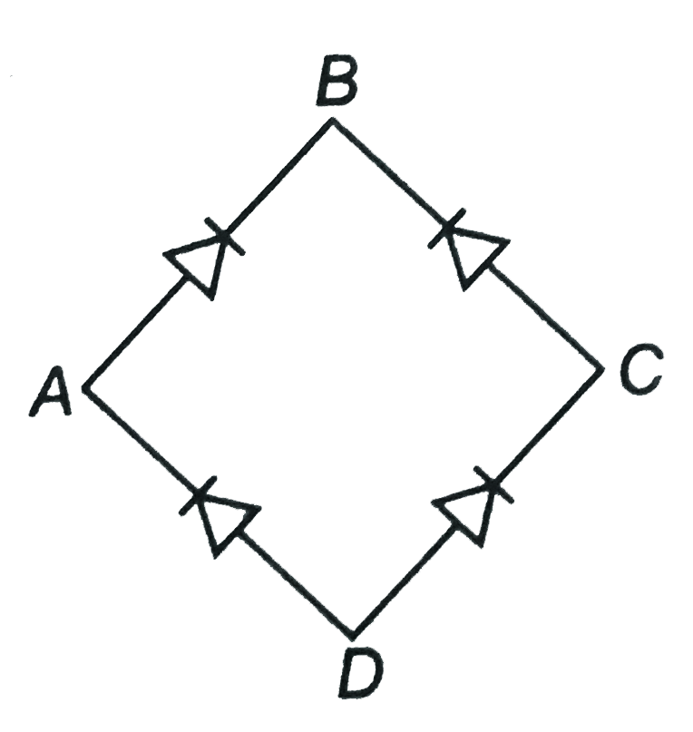
(a ) zero
( b) same as the input
( c) full - wave rectified
(d) half - wave rectified .
View SolutionAn oscillator is nothing but an amplifier with
View SolutionWhen a p-n junction diode is reverse biased the flow of current across the junction is mainly due to
View SolutionThe part of a transistor which is most heavily doped to produce large number of majority carriers is
View SolutionA piece of copper and the other of germanium are cooled from the room temperature to 80 K, then which of the following would be wrong statements?
View SolutionDiamond is very hard, because
View SolutionFor an electronic valve, the plate current I and plate voltage V in the space charge limited region are related as
View SolutionWhich one of the following is the weakest kind of the bonding in solids ?
View SolutionFor amplification by a triode, the signal to be amplified is given to
View SolutionThe following truth table corresponds to the logical gate

View SolutionTo use a transistor as an amplifier
View SolutionThe depletion layer in `P-N` junction region is caused by
View SolutionIn a common base ampifier , the phase difference between the input signal and output voltage is
View Solution
Exercise questions and complete solutions for chapter SOLID AND SEMICONDUCTOR DEVICES of NEET PREVIOUS YEAR (YEARWISE + CHAPTERWISE) of Class 12