Complete Solutions to PROBLEMS FOR PRACTICE of chapter ELECTRONIC DEVICES of Class 12 book with complete answers and questions
| Class 12 | PHYSICS |
| Chapter | ELECTRONIC DEVICES |
| PRADEEP | PROBLEMS FOR PRACTICE |
| Number Of Questions | 7 |
| Academic Year | 2023-24 |
A doped semiconductor has impurity levels 30meV bleow the conduction band,(a)Is the material m-type or p-type? (b)In a thermal collision,and amount kT of energy is given to the extra electron loosely bound to the impurity ion and this electron is just able to jump into the conduction band. Calculate the temperature T.
View SolutionA battery of emf `2V` is connected across a block of length `0.1m` and area of cros-section `1xx10^(-4)m^(2)`. If the block is of intrinsic silocon at `300K`, find the electron and hole currents. What will be the magnitude of the total current? What will be the magnitude of the total current if germanium is used instead of silicon?
Given that for `Si` at `300K`: `mu_(e)=0.135m^(2)V^(-1)s^(-1),mu_(h)=0.048m^(2)V^(-1)s^(-1)` and intristic carrier concentration `n_(i)=1.5xx10^(16)m^(-3)`. For `Ge` at `300K: mu_(e)=0.39m^(2)V^(-1)s^(-1),mu_(h)=0.19m^(2)V^(-1)s^(-1)` and `n_(i)=2.4xx10^(19)m^(-3)`
View SolutionA potential barrier of `0.7V` exists across a p-n junction If the depletion layer is `7.0xx10^(-7)m` thick, what is the intensity of the electric filed in this region? If an electron is approaching the p-n junction from the n-side with a speed `6.0xx10^(5)ms^(-1)`, determine the speed with which it enters the p-side of p-n junction.
View SolutionThe following data was obtained for a given transistor

For this data, calculate the input resistance of the given transistor.
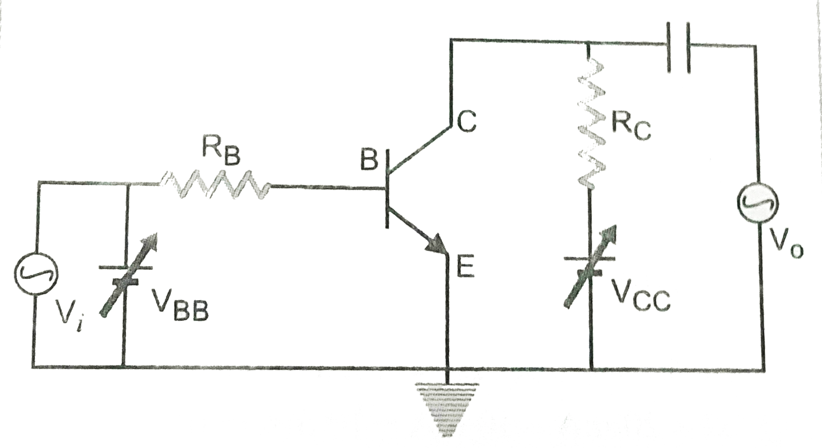
View SolutionFor a CE-transistor amplifier Fig.the audio signal voltage across the collector resistance of `1.0kOmega` is `1.0V`. Suppose the current amplification factor of the transistor is 100, what should be the value of `R_(B)` in series with `V_(BB) =0.6V`. Also calculate the voltage drop across the collector resistance.

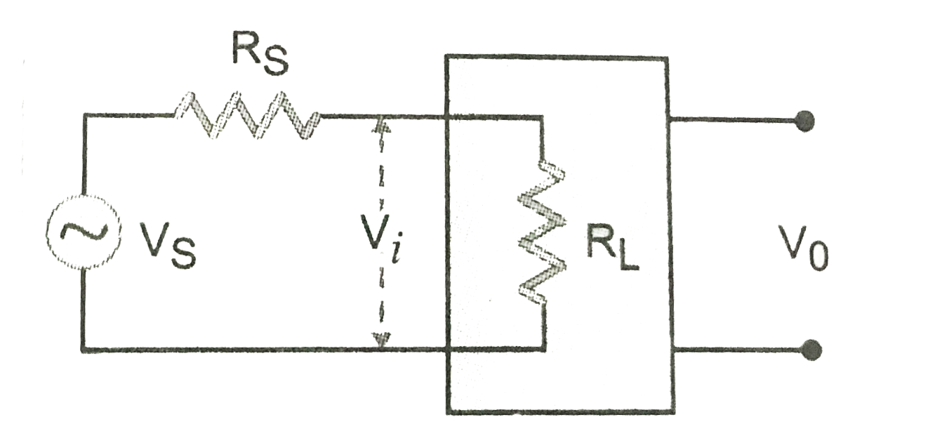
View SolutionAn amplifier is represented by the circuit shown in Fig. Here `r_(i)` is the input resistance of the amplifier and the voltage `V_(i)` is appearing across it. This voltage is amplified by a factor `A_(V)` and appears across the load as voltage `V_(0)`

An external voltage `V_(s)` is applied at the input terminals of the amplifier via series resistance `R_(S)`. What will be the apparent gain `A_(V)(=V_(0)//V_(s))` of the ampilifier in terms of `A_(V), R_(S)` and `r_(i).`
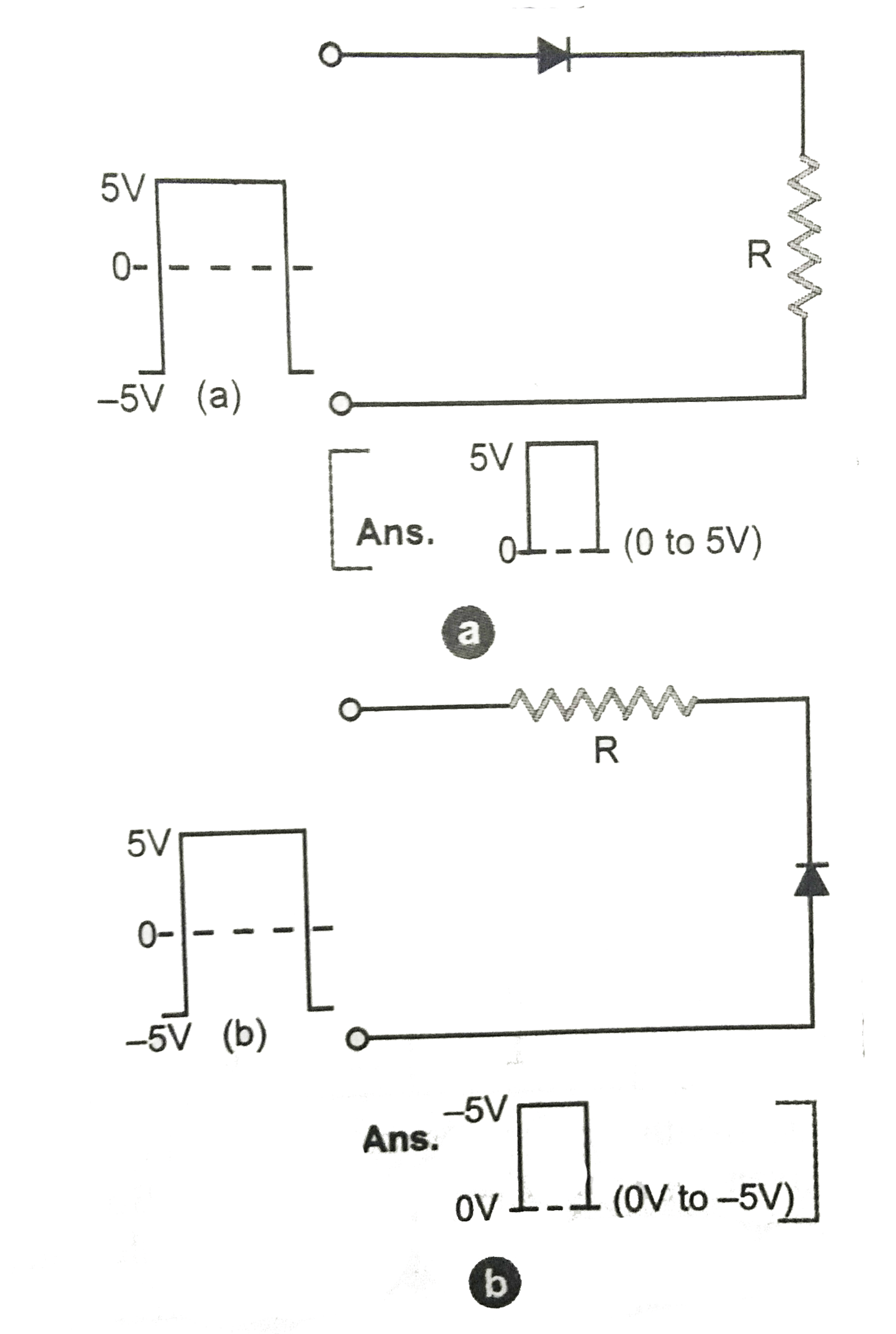
View SolutionIn the following circuit, if the input wave form is as shown in the figure, what will be the wave form (i) across R in Fig. and (ii) across the diode in Fig. Assume that the diode is ideal.

View Solution
PROBLEMS FOR PRACTICE questions and complete solutions for chapter ELECTRONIC DEVICES of PRADEEP PHYSICS (HINGLISH) of Class 12
All Exercises from PRADEEP Class 12 PHYSICS ELECTRONIC DEVICES
- ADVANCED PROBLEMS FOR COMPETITIONS
- CONCEPTUAL PROBLEMS
- Exercise
- EXERCISES (NCERT)
- Fill in the Blanks
- HIGHER ORDER THINKING SKILLS
- INTEGER TYPE QUESTION
- LONG QUESTION ANSWER
- LONG QUESTION ANSWER (NCERT)
- MCQ
- MULTIPLE CHOICE QUESTIONS
- PROBLEMS FOR PRACTICE
- SAMPLE PROBLEM
- SHORT QUESTION ANSWER
- Solved Examples
- VERY SHORT QUESTION ANSWER (NCERT)