Complete Solutions to Solved Examples of chapter ELECTRONIC DEVICES of Class 12 book with complete answers and questions
| Class 12 | PHYSICS |
| Chapter | ELECTRONIC DEVICES |
| PRADEEP | Solved Examples |
| Number Of Questions | 100 |
| Academic Year | 2023-24 |
A silicon specimen is made into a `P`-type semiconductor by dopping, on an average, one helium atoms per `5xx10^(7)` silicon atoms. If the number density of atoms in the silicon specimen is `5xx10^(28) at om//m^(3)` then the number of acceptor atoms in silicon per cubic centimeter will be
View SolutionThe number density of electrons and holds in pure silicon at `27 ^(@)C` are equal and its value is `2.0xx10^(16)m^(-3)`. On doping with indium, the hole density increases to `4.5xx10^(22)m^(-3)`, find the electron density in doped silicon.
View SolutionThe densities of electrons and holes in an extrinsic semiconductor are `7.5xx10^(13)cm^(-3)` and `4.5 xx 10^(12)cm^(-3)` respectively. The mibilities of electrons and holes are `23xx10^(3)cm^(2)//V-s` and `10^(2)cm^(2)//V-s` respectively. What is the type of semiconductor? Find the resistivity of this semiconductor.
View SolutionIn a p-n junction diode the reverse saturation current is `10^(-5)A` at `27^(@)C`. Find the forward current for a voltage of `0.2 V`. Given exp. `(7.62)=2038.6,k=1.4xx10^(-23)JK^(-1)`.
View SolutionIn a n-p-n transister circuit the collector current is `9 mA`. If `90%` of the electrons emitted reach the collector, find emitter current and base current
View SolutionIn a transistor when base-emitter voltage is changed from `0.6 V` to `0.8 V`, the change in base current is `500 muA` to the change in collector current is `10 mA` to `40 mA`, when the collector-emitter voltage is kept constant at `2 V`. Find input impendance forward current ratio:
View SolutionIn a common base circuit, the current gain is `0.96`. If the base current is `60 mu A`, find the emitter current and collector current.
View SolutionFor a common base amplifier, if the values of resistance gain and voltage gain are `3000` and `2800` respectively, find the current gain and power gain of this amplifier.
View SolutionThe current gain for common emitter amplifier is `59`. if the emitter current is 6.0mA, find the base of current and collector current
View SolutionConvert binary number `10111` into decimal number.
View SolutionConvert binary number `1010` into decimal number.
View SolutionDetermine the binary equivalent of `(0.25)_(10)`.
View SolutionDetermine the binary equivalent of `(6.25)_(10)`.
View SolutionFind the fractional decimal number of `(0.101)_(2)`.
View SolutionLet us add `(110010)_(2)` and `(111101)_(2).`
View SolutionLet us add `(10101)_(2)` and `(1011)_(2)`
View SolutionLet us find the difference of `(111101)_(2)` and `(110010)_(2)`
View SolutionFind the maximum wave- length of electromagnatic radiation which can creat a hole-electron pair in silicon. The band is silicon is `1.1 eV`. [Use `h = 6.6xx10^(-34) Js , c=3xx10^(8)ms^(-1), e=1.6xx10^(-19)C]`
View SolutionThe mean free path of conduction electrons in copper is about `4 xx 10^(-8)m`. Find the electric field which can give, on an avrage, `2 eV` energy to a conduction electron in a block of copper.
View SolutionIn a pure semiconductor, the number of conduction electron is `6xx10^(19)` per cubic metre of size `1 cm xx 1 cmxx2mm`?
View SolutionA semiconductor has equal electron and hole concentration of `2 xx 10^(8)m^(-3)`. On doping with a certain impurity, the hole concertraction increases to `4 xx 10^(10)m^(-3)`. (i) What type of semiconductor is obtained on doping? (ii) Calculate the new electron hole concentration of the semiconductor. (iii) How does the energy gap very with doping?
View SolutionSuppose a pure Si-crystal has `5xx10^(28) "atoms" m^(-3)`. It is doped by 1 ppm concentration of pentavalent As. Calculate the number of electrons and holes. Give that `n_(i)=1.5xx10^(16)m^(-3)`.
View SolutionSuppose the energy liberated in the recombination of a hole-electron pair is converted into electromagnatic radiation. If the maximum wavelength emitted is 660nm, what is the band width? (Use `h=6.6xx10^(-34) J-s)`
View SolutionFind the maximum wavelength of electromagnatic radiation which can creat a hole-electron pair in silicon. The band is silicon is `1.1 eV`. [Use `h = 6.6xx10^(-34) Js , c=3xx10^(8)ms^(-1), e=1.6xx10^(-19)C.`
View SolutionA semiconductor is made extrinsic by adding trivalent impurity. The resulting p-type semiconductor should be of conductivity `12 mho m^(-1)`. Mobility of holes is `400 cm^(2)V^(-1)s^(-1)`. Neglecting electron contribution find the number density of accetor atoms. charge on an electron`= 1.6xx10^(-19) C`.
View SolutionA semiconductor is known to have an electron concentration of `5xx10^(12) cm^(-3)` and a hole concentration `8xx10^(13)cm^(-3) ` Is the semi-conductor n-type or p-type? What is the resistivity of the sample, if the electron mobility is `23,000 cm^(2) V^(-1)s^(-1)`? Take charge on electron, `e=1.6xx10^(-19) C`.
View SolutionA p-n junction when forward biased has a drop of `0.6 V` which is assumed to be independent of current. The current in excess of `10 mA`through the diode produces a large joule heating effect which burns the diode. If we want to use `1.5 V` battery to forward bias the diode, what should be the value of resistor used in series with the diode so that the maximum current does not exceed 6 mA?
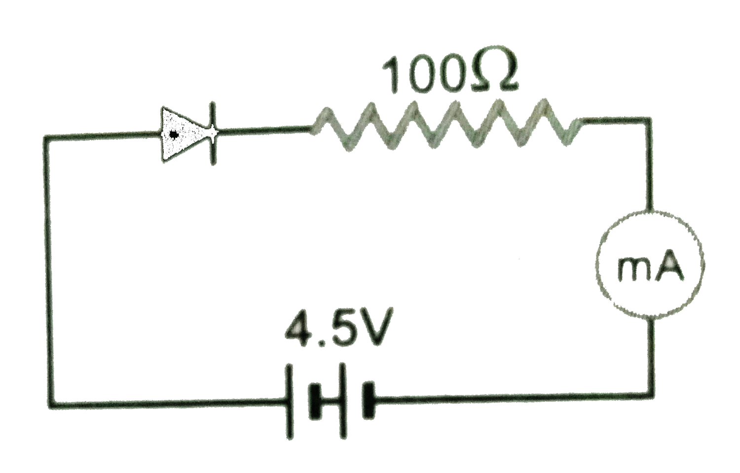
View SolutionFigure Shows a diode connected to an external resistance and an e.m.f. Assuming that the barrier potential developed in diode is `0.5 V`, obtain the value of current in the circuit in milliampere.
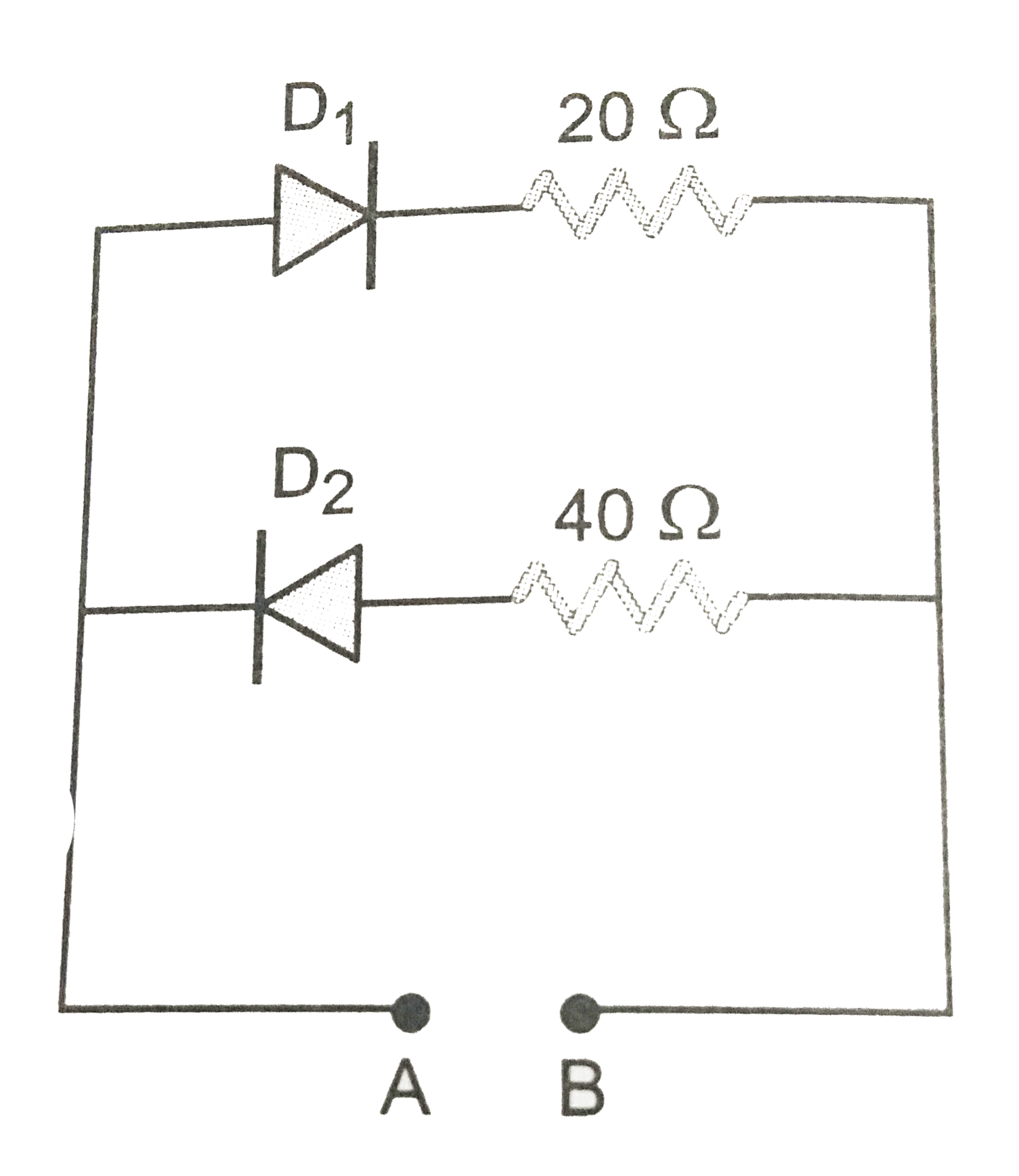
View Solution`A` battery of `1.5 V` may be connected across the point `A` and `B` as shown in Fig . What is the current drawn from the battery if the positive terminal of the battery is connected to `` the point `A` and `` the point `B`. The junction diodes `D_(1)` and `D_(2)` used are ideal diodes.
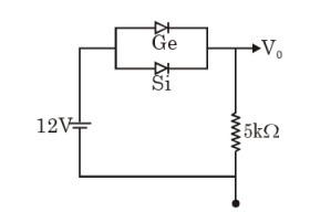
View SolutionCalculate the value of output voltage `V_(0)` (in V) if the Si diode and Ge diode conduct at `0.7V` and `0.3 V` respectively. Fig.
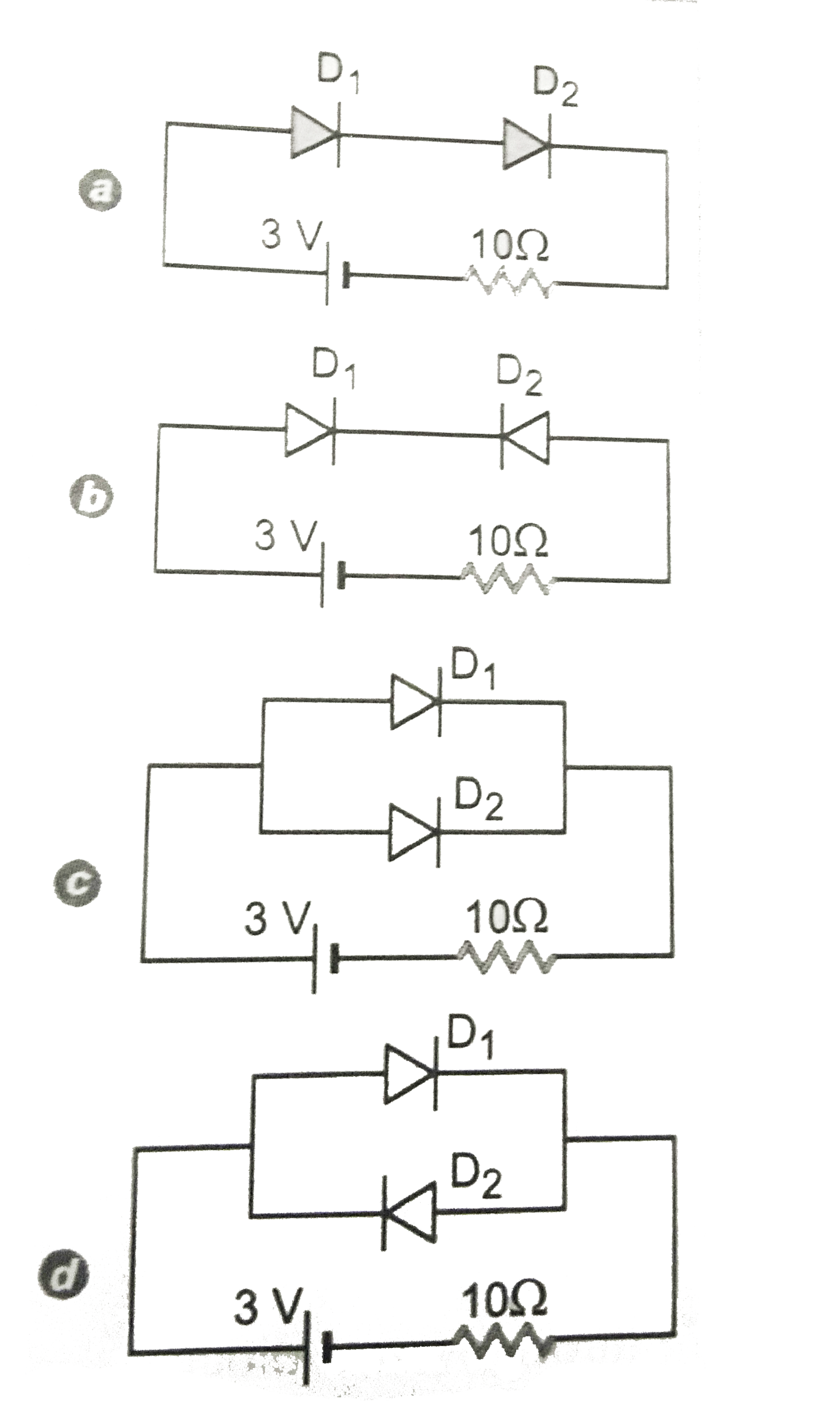
View SolutionFind the total current in the circuits shown in Fig. , , and . Each diode used is ideal
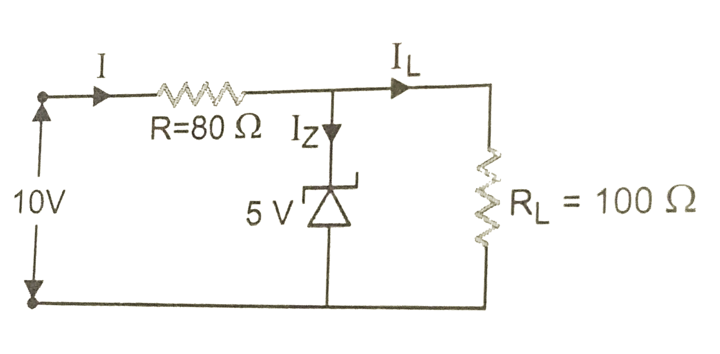
View SolutionIn the Fig. find out the current passing through `R_(L)` and zener diode.
View SolutionA full wave rectifier uses two diodes, the internal resistance of each diode may be assumed constant at `25Omega`. The transformer r.m.s. secondary voltage from centre tap to each end of the secondary is `50 V` and load current (ii) the rms value of load current.
View SolutionIn a full wave junction diode rectifier, the input a.c. voltage has r.m.s. value of `10 V`. The transformer used is a step up one having transformation ratio `1: 2`. Calculate the D.C. voltade in the recitified output
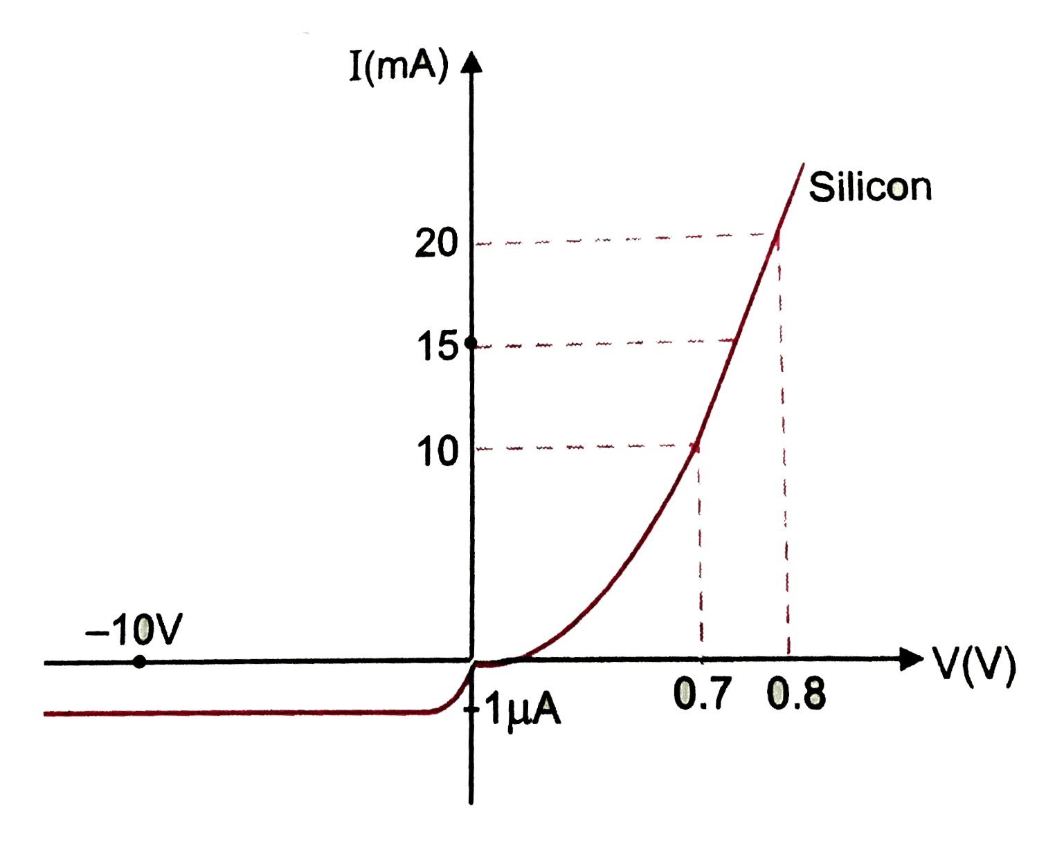
View SolutionThe V-I characteristics of a silicon diode is shown in the Fig. . Calculate the resistsnce of the diode at `I_(D)=15mA` and ` V_(D)=-10V`.
View SolutionIn a zener regulated power supply a zener diode with
` V_z = 6.0 V` is used for regualtion. The load current is to eb 4.0 mA and the
unregulated input is 10.0 V . What should be the value of series resistor R?
View SolutionA `6V` zener diode along with a series resistance `R` is connected accrose a `12 V` supply. Calculate the minimum value of the resistance `R` required, if the maximum zener current is `30 mA`.
View SolutionThe current gain in common emitter amplifier is `59`. If the emitter current is `6.0mA`, find, (i) base current (ii) collector current.
View SolutionIn p-n transistor circuit, the collector current is `10 mA`. If `90%` of the holes reach the collector, find emitter and base currents.
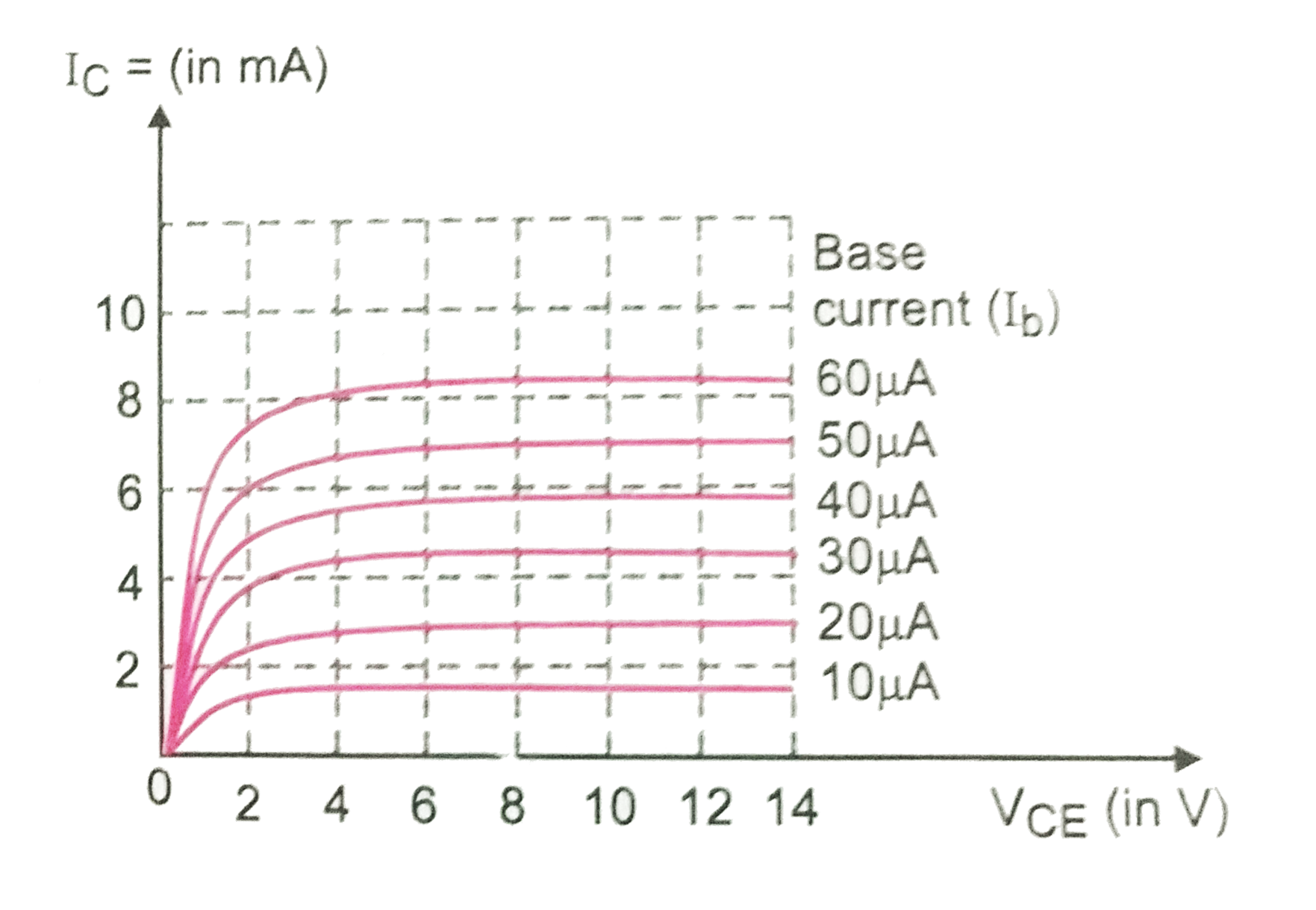
View SolutionFrom the output characteristics of common emitter circuit shown in Fig., calculate the value of `beta_(ac)` and `beta_(dc)` of the transistor when `V_(cE)` is `10 V` and `I_c =4.0mA`.
View SolutionThe potential difference across the collector of a transistor, used in common emitter mode is `1.5V`, with the collector resistance of `3 kOmega`. Find (i) the emitter current and (ii) the base current, if d.c. gain of the transistor is 50.
View SolutionA transistor has a current gain of 50. If the collector resistance `5kOmega`. Calculate the output voltage if input voltage is `0.01V`.
View SolutionFor a CE- transistor amplifier , the audio signal voltage across the collector resistance of ` 2 k Omega ` is 2 V . Suppose the current amplifiaction factor of the transistor is 100 . Find the input signal voltage and base current , if the base resistance is `1 k Omega` .
View SolutionThe current gain of a transistor in a common base arrangement is `0.95`. Find the voltage gain and power gain if the load resistance of output circuit is `400kOmega` and the input resistance is `200Omega`.
View SolutionIn a silicon transistor, a change of `7.89 mA` in the emitter current produce a change of 7.8 mA in the collector current. What change in the base current is necessary to produce an equivalent change in the collector current?
View SolutionFor a `CE` transistor amplifier, the audio signal voltage across the collector resistance of `2k Omega` is `2V`. Suppose the current amplification factor of the transistor is `100`. The value of `R_(B)` in series with `V_(BB)` supply of `2V`, if the `DC` base current has to be `10` times the signal current is.
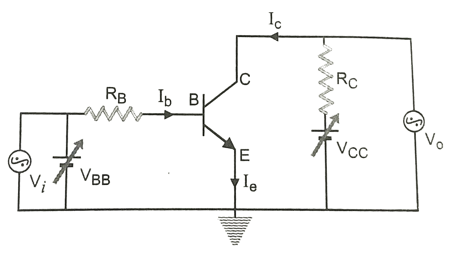
View SolutionIn common emitter transistor as shown in Fig., the `V_(BB)` supply can be varied from 0 V to 5.0V. The Si. Transistor has `beta_(ac)=250` and `R_(B)=100kOmega, R_(c)=1k Omega,V_(C C)=5.0V`. Assume that when the transistor is saturated, `V_(CE)=0V` and `V_(BE)=0.8V`. Calculate the minimum base current, for which the transistor will reach saturation. Hance, determine `V_(i)` when the transistor is 'switched on' find ranges of `V_(i)` for which the transistor is switched off and switched on.
View SolutionAn n - p- n transistor is connected in common - emitter configuraration in which collector supply is 8 V and the voltage drop across the load resistance of ` 800 Omega ` connected in the collector circuit is 0.8 V . If current amplification factor is 25 , determine collector - emitter voltage and base current . If the internal resistance of the transistor is ` 200 Omega ` , calculate the voltage gain and the power gain.
View SolutionA potential barrier of 0.4V exists across a p-n junction. If the depletion region is `4.0xx10^(-7)m` wide, what is the intensity of the electric field in this region? If an electron with speed `4.5xx10^(5)m//s` approaches the p-n junction from the n-side, find the speed with which it will enter the p-side.
View SolutionIn an n-p-n transistor `10^(10)` electrons enter the emitter in `10^(-6)`s. If 2% of the electrons are lost in the base, find the current transfer ratio and the current amplification factor.
View SolutionAn amplifier is represented by the circuit shown in Fig. Here `r_(i)` is the input resistance of the amplifier and the voltage `V_(i)` is appearing across it. This voltage is amplified by a factor `A_(V)` and appears across the load as voltage `V_(0)`
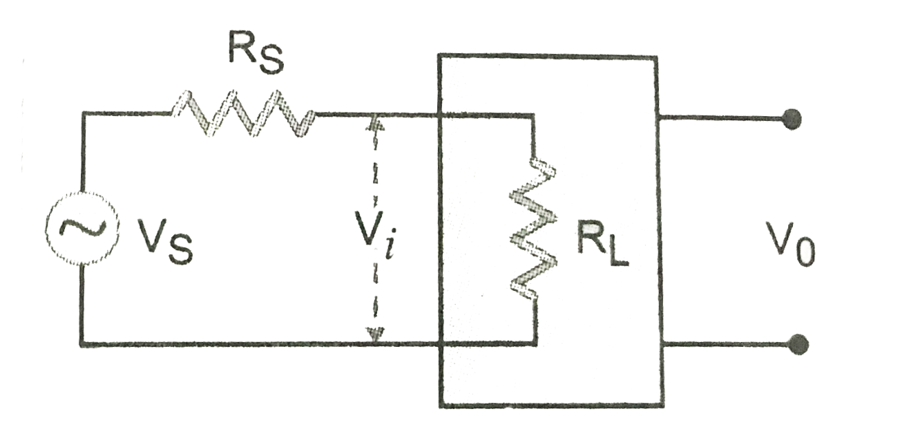
An external voltage `V_(s)` is applied at the input terminals of the amplifier via series resistance `R_(S)`. What will be the apparent gain `A_(V)(=V_(0)//V_(s))` of the ampilifier in terms of `A_(V), R_(S)` and `r_(i).`
View SolutionWhat is the decimal number of binary number `(111001.01)_(2)`?
View SolutionWhat is the binary additon of `(101010)_(2)` and `(010101)_(2)`?
View SolutionSubtract `(10101)_(2)` from `(111001)_(2)`.
View SolutionThe truth table shown below is for which of the following gates:
`{:(NaND,,A,B,Y),(AND,,1,1,0),(XOR,,1,0,1),(NOT,,0,1,1),(,,0,0,1):}`
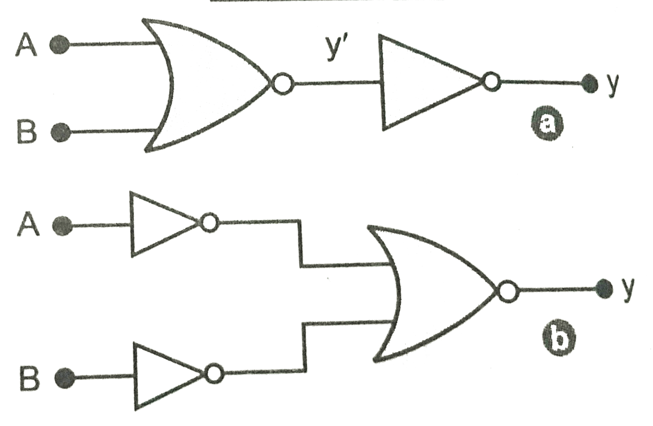
View SolutionYou are given the two circuits as shown in Fig. and . Show that circuit acts as OR gate while the circuit acts as AND gate.
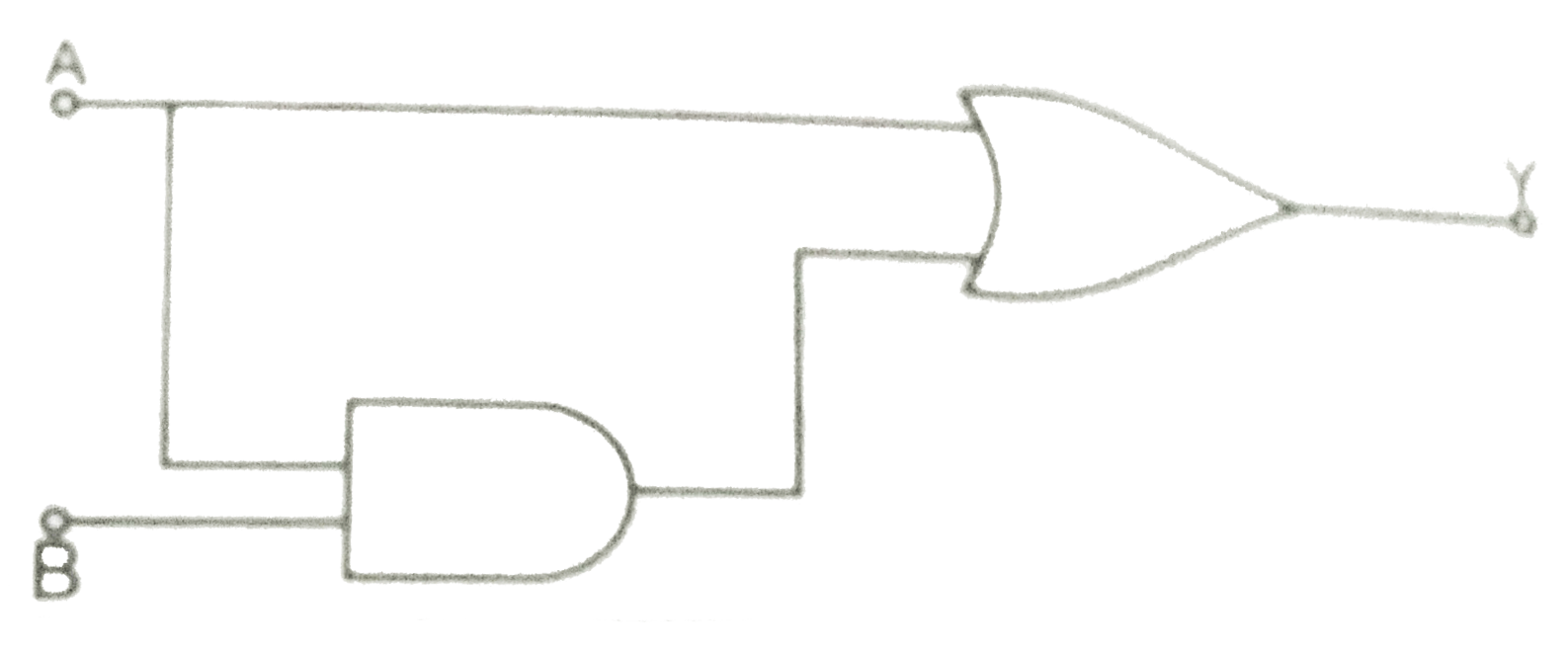
View SolutionExpress by a truth table, the output Y for all possible input A and B in the following circuit Fig.
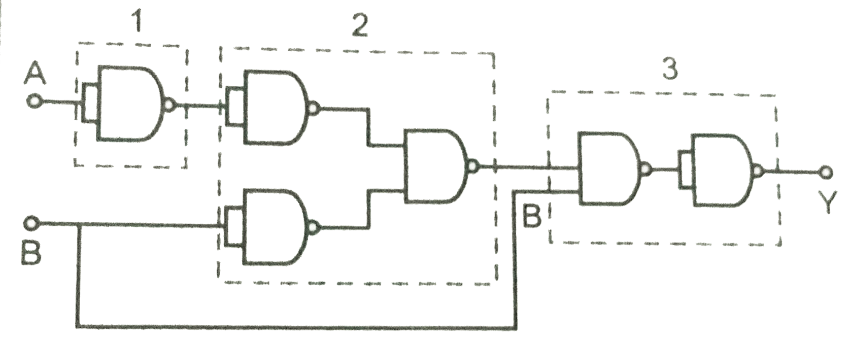
View SolutionIdentify which basic gate, OR, AND and NOT is represented by the circuits in the dotted line boxes 1, 2 and 3 Fig.
View SolutionLet A, B and C be any three logic variables, prove the following Boolean identity.
`A.B.C+A.barB.C+A.B.barC=A.(B+C)`
View SolutionA student has to use an appropriate number of (i) NAND gates (only) to get the output `y_(1)` (ii) NOR gates (only) to get the output `y_(2)` from two given input A and B as shown in the Fig.
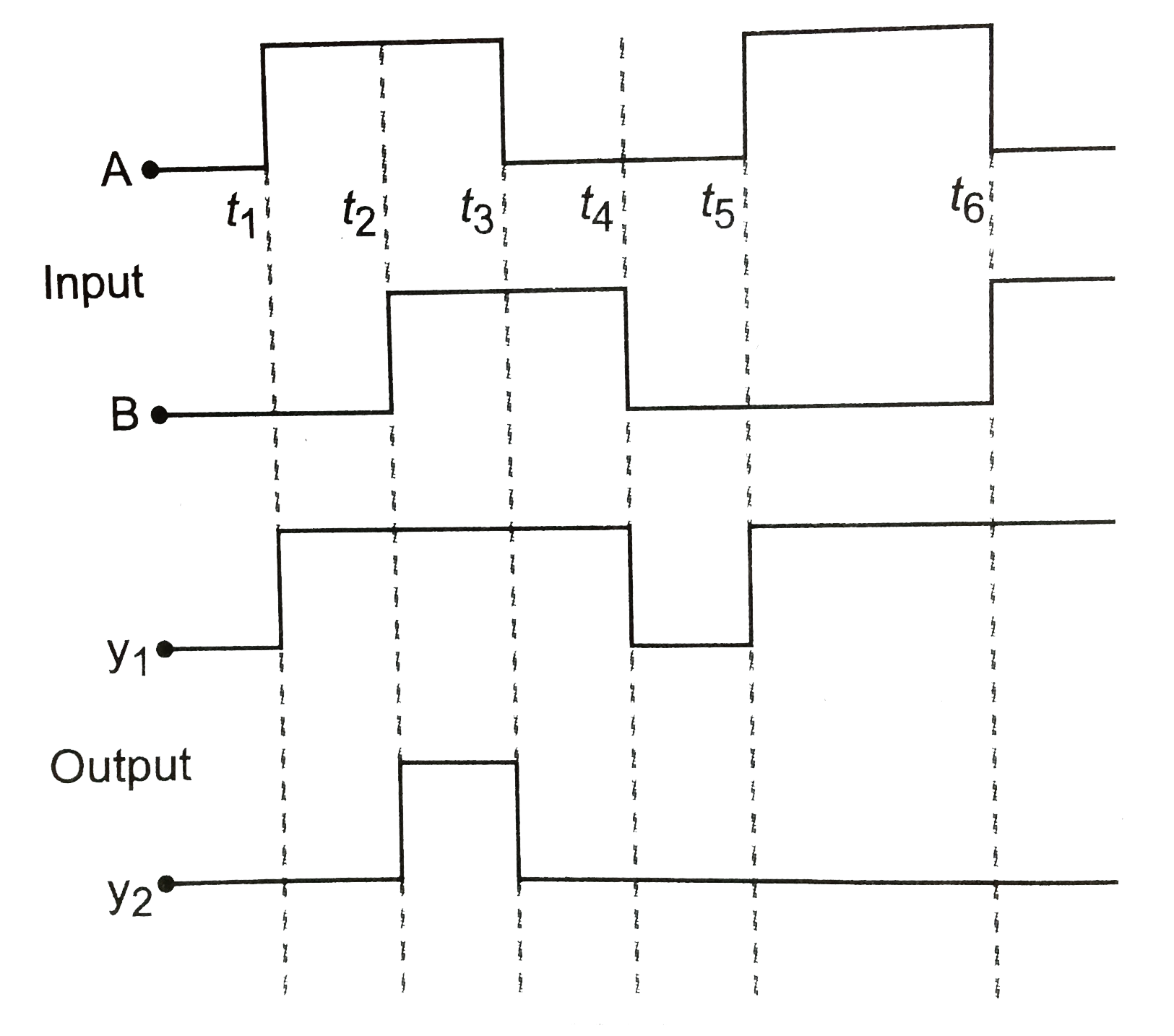
Identify the 'equivalent gate' needed in each case. Show how one can connect an appropriate number of (i) NAND (ii) NOR gates respectively in the two cases to gat the equivalent gates.
View SolutionThe metallic conductors are opaque. Why?
View SolutionOut of the ionic, covalent and metallic and van der Waal's solids, which will be widely used to produce a conductor, semiconductor and insulator?
View SolutionC, Si and Ge have same lattice structure. Why is C insulator,
while Si and Ge intrinsic semiconductors ?
View SolutionDiscuss the quantum states of sodium crystal having N atoms.
View SolutionAssertion : An `N`-type semiconductor has a large number of electrons but still it is electrically neutral.
Reason: An `N`-type semiconductor is obtained by doping an intrinsic semiconductor with a pentavelent impurity.
View SolutionA p-type semiconductor has a large number of holes but still it is electrically neutral. Explain.
View SolutionA doped semiconductor has impurity levels `40 me V` below the conductor band. Is the material n-type or p-type? In a thermal collision, an amount kT of energy is given to the extra electron loosely bound to the impurity ion and this electron is just able to jump into the conduction band. Calculate the temperature T. Given `k=8.62xx10^(-5) eV//K`.
View SolutionA hole created father below the top of valence band has higher energy than created at the top of valence band. Explain.
View SolutionThe resistance of p-n junction is low when forward biased and is high when reverse biased. Explain.
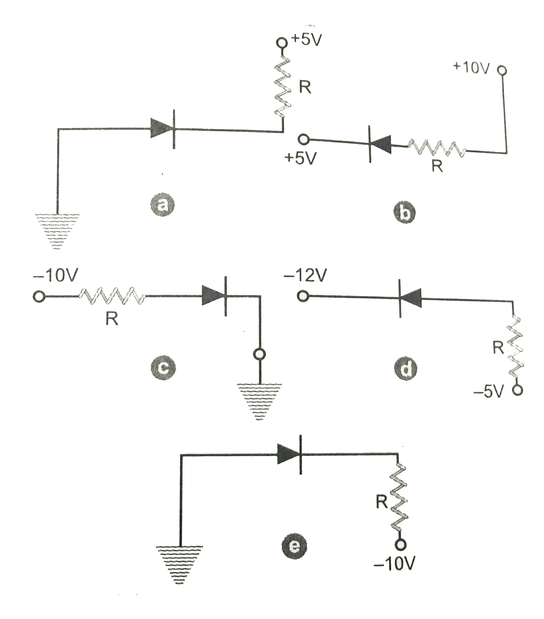
View SolutionIn the following Fig., , , and (e), which of the diode are forward biased and which are reverse biased and why?
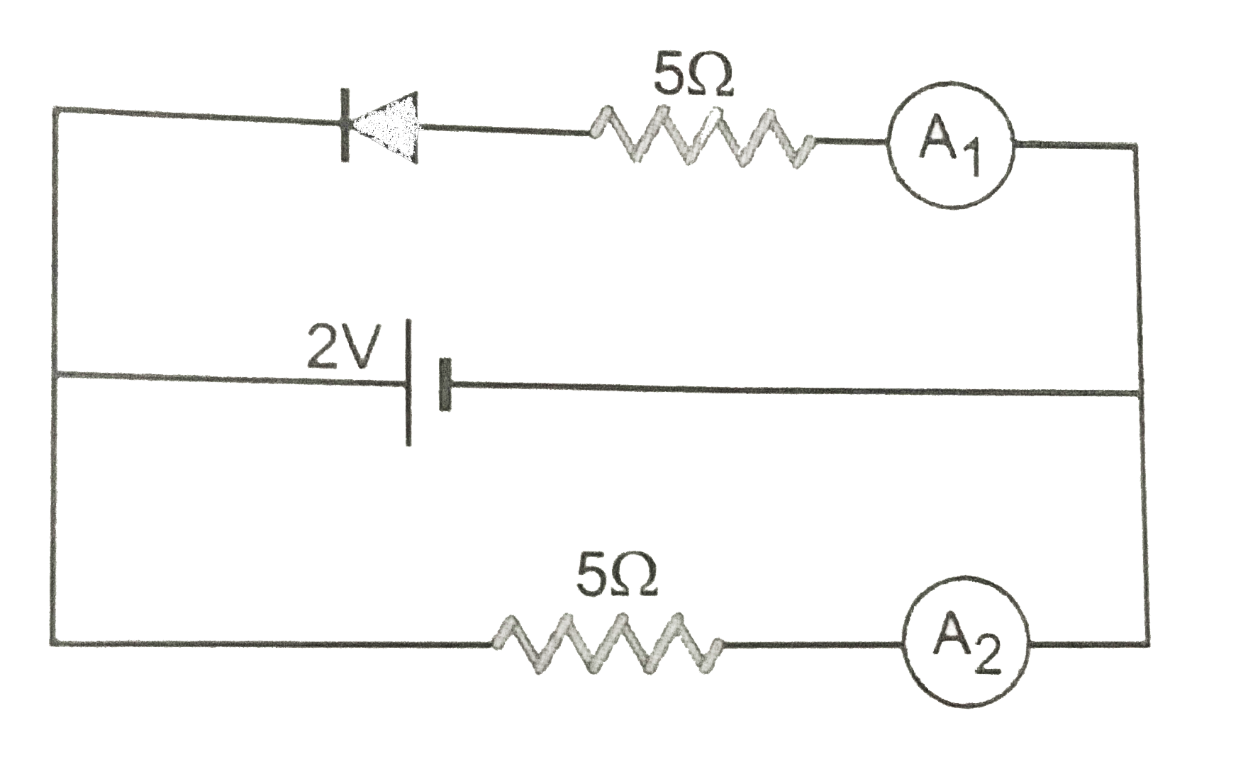
View SolutionWhat are the reading of ammeters `A_(1)` and `A_(2)` shown in Fig.? Neglect the resistances of the ammeters, when the p-n junction used is ideal one.
View SolutionWhy are Si and GaAs are preferred materials for solar cells?
View SolutionA zener diode has a contract potential of `0.8 V` in the absence of biasing. It undergoes zener breakdown for an electric field of `10^(6) Vm^(-1)` at the depletion region of p-n junction. If the width of the depletion region is 2-4mu m, what should be the reverse biased potential for the zener breakdown to occur?
View SolutionThe applied input a.c. power to a half wave retifier I 100 watt. The d.c. output power obtained is 40 watt. (i) What is the rectification efficiency and (ii) What is the power efficiency?
View SolutionDetermine the current through the resistancees of the circuit shown in Fig.. The each p-n junction used is ideal one.
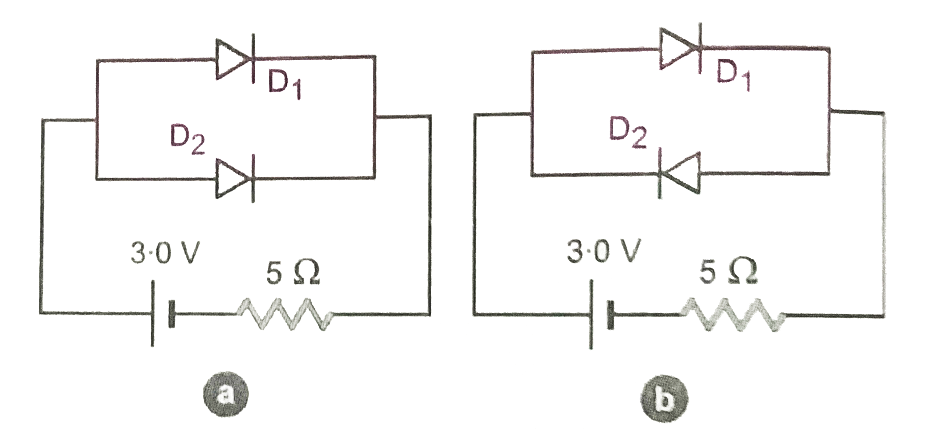
View SolutionA 3V battery may be connected across the point A and B as shown in Fig. Assume that the resistance of each diode is zero in the forward bias and infinity in the reverse bias. Find the current supplied by the battery if the positive terminal of the battery is connected to the point A the point B.
View SolutionHow reverse current suddenly increase at the breakdown voltage in case of zener diode?
View SolutionWhat do the acronyms LASER and LED stands for? Name the factor which determines (i) frequency and (ii) intensity of light emitted by LED.
View SolutionIn V-I characteristics of a p-n junction diode, why is the current under reverse bias almost independence of the applied potential upto a critical voltage?
View SolutionIn a transistor base is made thin and doped with little impurity atoms. Why?
View SolutionWhat will happen if emitter be reversebiased and collector be forward biased in a transistor?
View SolutionWhat will happen if both, emitter and collector of a transistor are reversed biased?
View SolutionWhat will happen if emitter as well as collector in a transistor are forward biased?
View SolutionTransistor is a temperature-sensitive device. Explain.
View SolutionA transistor is current operated device. Explain.
View SolutionExplain, why the input resistance of a transistor is low and output resistance is high.
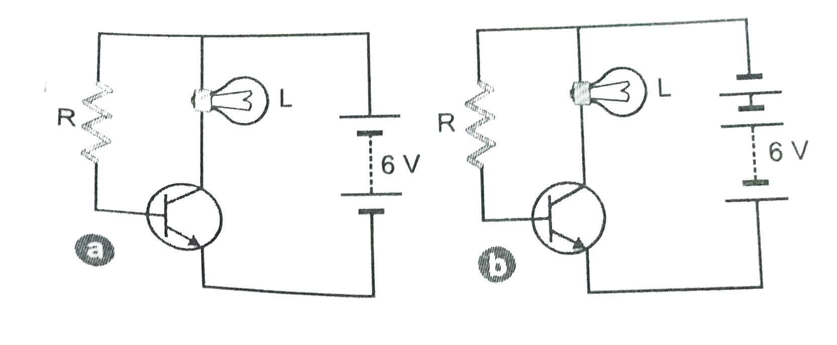
View SolutionIn only one of the circuits given below, the lamp L light. Which circuit is it ? Give reason for your answer.
View SolutionIf the base region of a transistor is made large, as compared to a usual transistor, how does it affect (i) the collector current and (ii) current gain of this transistor.
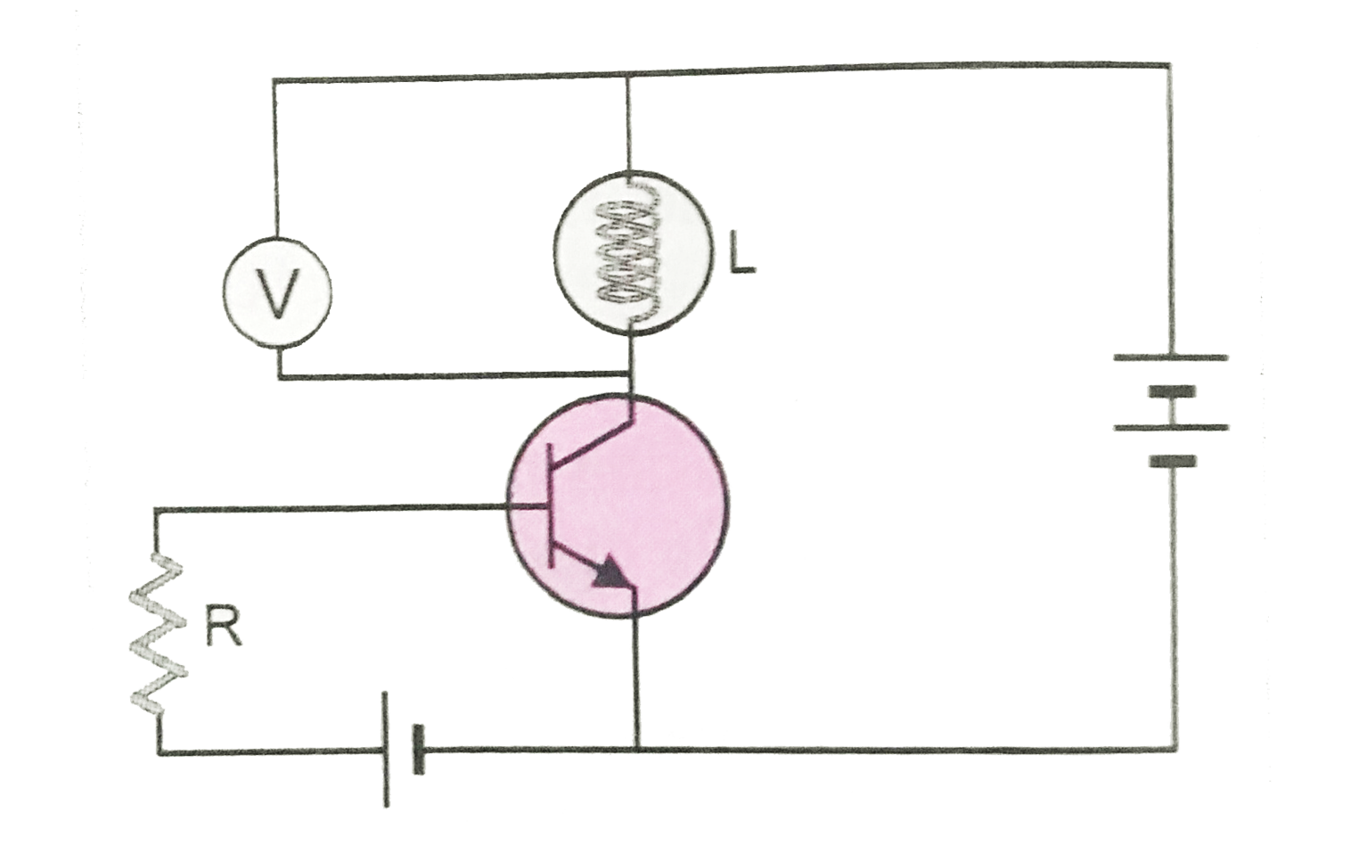
View SolutionIn the circuit shown in Fig.a voltage V is connected across lamp L. What changes would occur at lamp and the voltage V, if the resistance R is reduced in value?
View SolutionIs the voltage gain of a common-emitter ampilifier constant, irrespective of the magnitude of the input signal? Give reason.
View SolutionHow will you test in a simple way whether a transistor is spoiled or in working order?
View SolutionAssertion: `NAND` or `NOR` gates are called digital building blocks.
Reason: The repeated use of `NAND` (or `NOR`) gates can produce all the basic or complicated gates.
View SolutionDiscuss how a NOT gate is realised using NAND gates.
View SolutionDicuss how the AND gate is realised from the NAND gate.
View SolutionDicuss how the OR gate is realised from the NAND gate.
View SolutionDicuss how the OR gate is realised from the NOR gate.
View SolutionDicuss how the AND gate is realised from the NOR gate.
View SolutionThe output of a two NAND gates is fed as input to an OR gate. Write the truth table for the final output of combination. Name this new logic gate.
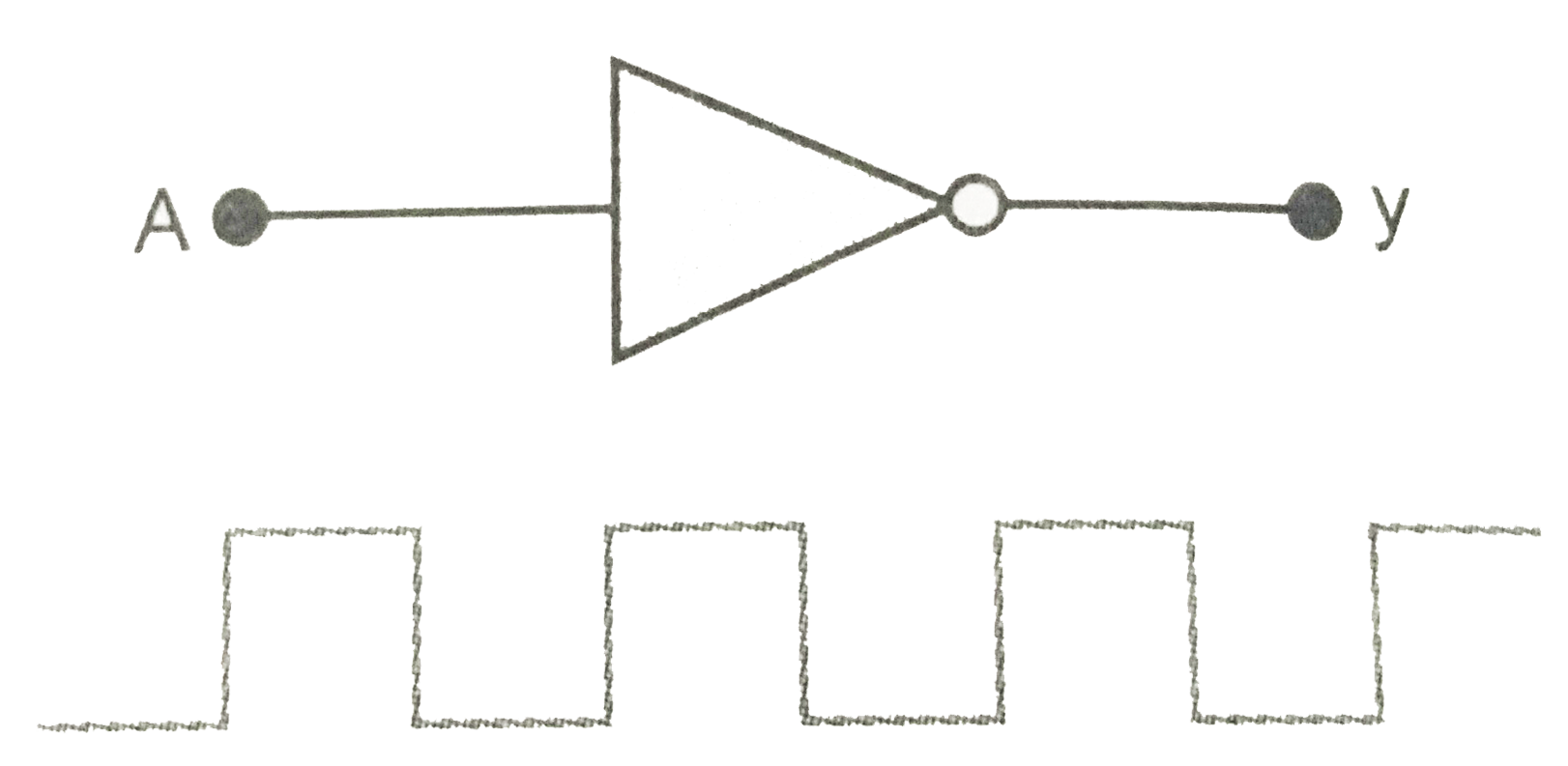
View SolutionIn Fig., circuit of a logic gate and input waveform is shown. (i) Name the logic gate (ii) Write its truth table and (iii) give the output wavefrom.
View SolutionIdentify the logic gates marked P and Q in the circuit Fig. Write the truth table for this combination.

View Solution
Solved Examples questions and complete solutions for chapter ELECTRONIC DEVICES of PRADEEP PHYSICS (HINGLISH) of Class 12
All Exercises from PRADEEP Class 12 PHYSICS ELECTRONIC DEVICES
- ADVANCED PROBLEMS FOR COMPETITIONS
- CONCEPTUAL PROBLEMS
- Exercise
- EXERCISES (NCERT)
- Fill in the Blanks
- HIGHER ORDER THINKING SKILLS
- INTEGER TYPE QUESTION
- LONG QUESTION ANSWER
- LONG QUESTION ANSWER (NCERT)
- MCQ
- MULTIPLE CHOICE QUESTIONS
- PROBLEMS FOR PRACTICE
- SAMPLE PROBLEM
- SHORT QUESTION ANSWER
- Solved Examples
- VERY SHORT QUESTION ANSWER (NCERT)