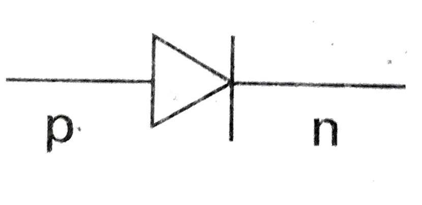
What is p-n junction diode ? Define depletion layer. Solution in Telugu
Whan an intrisic semiconductor crystal is grown with one side doped with trivalent element and on the other side doped with pentavalent element, a junction is formed in the crystal.It is called p-n junction diode.
A thin narrow region is formed on either side of the p-n junction,which is free from cahrge carriers is called depletion layer.

Topper's Solved these Questions
- BOOK - VIKRAM PUBLICATION ( ANDHRA PUBLICATION)CHAPTER - SEMICONDUCTOR ELECTRONICS : MATERIALS , DEVICES , AND SIMPLE CIRCUITS EXERCISE - SHORT ANSWER QUESTIONS16videos
SEMICONDUCTOR ELECTRONICS : MATERIALS , DEVICES , AND SIMPLE CIRCUITS
- BOOK - VIKRAM PUBLICATION ( ANDHRA PUBLICATION)CHAPTER - SEMICONDUCTOR ELECTRONICS : MATERIALS , DEVICES , AND SIMPLE CIRCUITS EXERCISE - LONG ANSWER QUESTIONS7videos
SEMICONDUCTOR ELECTRONICS : MATERIALS , DEVICES , AND SIMPLE CIRCUITS
- BOOK - VIKRAM PUBLICATION ( ANDHRA PUBLICATION)CHAPTER - SEMICONDUCTOR ELECTRONICS : MATERIALS , DEVICES , AND SIMPLE CIRCUITS EXERCISE - PROBLEMS4videos
SEMICONDUCTOR ELECTRONICS : MATERIALS , DEVICES , AND SIMPLE CIRCUITS
- BOOK - VIKRAM PUBLICATION ( ANDHRA PUBLICATION)CHAPTER - RAY OPTICAL AND INSTRUMENTSEXERCISE - TEXTUAL EXERCISES60videos
RAY OPTICAL AND INSTRUMENTS
- BOOK - VIKRAM PUBLICATION ( ANDHRA PUBLICATION)CHAPTER - TELANGANA MARCH-2019EXERCISE - SECTION -B5videos
TELANGANA MARCH-2019
Similar Questions
What are n-type and p-type semiconducts ?How is a semiconductor junction formed ?
02:24View SolutionWhat is a junction diode ? Explain the formation of depletion region at the junction. Explain the variation of depletion region in forward and reverse-biased condition.
03:27View SolutionIn a half wave rectifier, a p-n junction diode with internal resistance 20 ohm is used. If the load resistance of 2 ohm is used in the circuit, then find the efficiency of this half wave rectifier.
02:56View SolutionA small candal, 2.5 cm in size is placed at 27 cm in front of a concave mirror of radius of curvature 36 cm. At wht distance from the mirror should a screen be placed in order to obtain a sharp image ? Describe the nature and size of the image. If the candale is moved closer to the mirror, how would the screen have to be moved ?
03:02View SolutionExplain the formation of Mirage .
View SolutionIn a P−N junction diode is P region is heavily doped than n region then the depletion layer is
01:30View SolutionWhen the p−n junction diode is reverse biased, the thickness of the depletion layer
03:01View SolutionIn the depletion region of an unbiased p-n junction diode there are
View SolutionThe knee voltage of a p-n junction diode is 0.8 V and the width of the depletion layer is 2muA . The electric field in the depletion layer is
01:25View SolutionWhen a p-n junction diode is reverse biased, the thickness of the depletion layer
01:04View SolutionWhen a p-n junction diode is reverse biased, the thickness of the depletion layer
03:09View SolutionIn the depletion region of an unbiased p-n junction diode, there are
04:16View SolutionIn the depletion region of the an unbaised p-n junction diode, there are
View SolutionDepletion layer of unbiased p-n junction diode contains.....
View SolutionIn the depletion region of an unbiased p-n junction diode there are
View Solution

