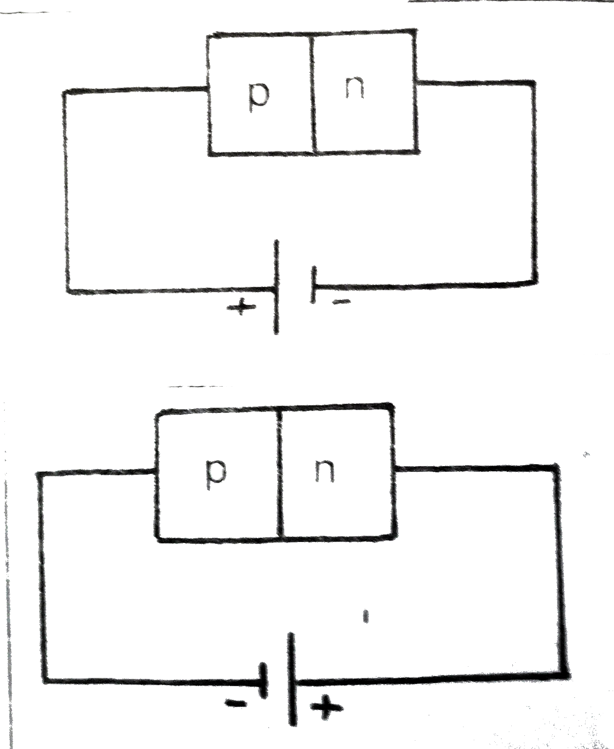
How is a battery connected to a junction dioide in (i) forward and (ii) reverse bias ?
(i) In p-n junction diode,if p-side is connected to positive terminal of a cell and n-side to negative terminal,it is called forward bias.
(ii) In a p-n junction diode, p-side is connected to negative terminal of a cell and n-side to positive terminal, it is called reverse bias.

Topper's Solved these Questions
- SEMICONDUCTOR ELECTRONICS : MATERIALS , DEVICES , AND SIMPLE CIRCUITS BOOK - VIKRAM PUBLICATION ( ANDHRA PUBLICATION)CHAPTER - SEMICONDUCTOR ELECTRONICS : MATERIALS , DEVICES , AND SIMPLE CIRCUITS EXERCISE - SHORT ANSWER QUESTIONS
16 Videos
- SEMICONDUCTOR ELECTRONICS : MATERIALS , DEVICES , AND SIMPLE CIRCUITS BOOK - VIKRAM PUBLICATION ( ANDHRA PUBLICATION)CHAPTER - SEMICONDUCTOR ELECTRONICS : MATERIALS , DEVICES , AND SIMPLE CIRCUITS EXERCISE - LONG ANSWER QUESTIONS
7 Videos
- SEMICONDUCTOR ELECTRONICS : MATERIALS , DEVICES , AND SIMPLE CIRCUITS BOOK - VIKRAM PUBLICATION ( ANDHRA PUBLICATION)CHAPTER - SEMICONDUCTOR ELECTRONICS : MATERIALS , DEVICES , AND SIMPLE CIRCUITS EXERCISE - PROBLEMS
4 Videos
- RAY OPTICAL AND INSTRUMENTSBOOK - VIKRAM PUBLICATION ( ANDHRA PUBLICATION)CHAPTER - RAY OPTICAL AND INSTRUMENTSEXERCISE - TEXTUAL EXERCISES
60 Videos
- TELANGANA MARCH-2019BOOK - VIKRAM PUBLICATION ( ANDHRA PUBLICATION)CHAPTER - TELANGANA MARCH-2019EXERCISE - SECTION -B
5 Videos
Similar Questions
(a). Explains briefly with the help of a circuit diagram how V-I characteristics of a p-n junction diode are obtainedin (i) forward bias, and (ii) reverse bias.
(b). A photo diode is fabricated from a semiconductor with a band gap of 2.8 EV. Can it detect wave length of 6000. nm? Justify.
View SolutionDraw the V-I characterisitics of p-n junction diode in forward bias and in reverse bias.
View Solution
Knowledge Check
A zener diode when used as a voltage regulator is connected in
(i) forward bias
(ii) reverse bias
(iii) parallel with the load resistance
(iv) series with the load resistanceAi and ii only are correctBii and iii only are correctConly i is correctDonly iv is correctReverse bias applied to a junction diode
ALowers the potential barrierBRaises the potential barrierCIncreases the majority carrier currentDIncreases the minority carrier currentReverse bias applied to a junction diode
ALower the potential barrierBRaises the potential barrierCIncreases the majority carriers currentDIncreasess the minority carrier current
Using the necessary circuit diagrams, show how the V-I characteristics of a p-n junction are obtained in
(i) Forward baising
(ii) Reverse biasing.
View SolutionReverse bias applied to a junction diode
View SolutionFor a reverse bias P-N junction-
View SolutionAssertion : The dominant mechanism for motion of charge carreis in forward and reverse biased silicon P-N junction are drit in both forward and reverse bias.
Reaon : In reverse biasing, no current flow through the junction.
View SolutionA Zener diode when used as a voltage regulator is connected
(a) in forward bias
(b) in reverse bias
( c) in parallel to the load
(d) in series to the load.
View Solution
