What is amplification ? Explain the working of a common emitter amplifier with necessary diagram.
Text Solution
Amplification : The process of raising the strength of a weak signal is called amplification and the device which accomplishes this job is called an amplifier.
Amplifiers are of two types. (1) Power amplifier (2) Voltage amplifier.
Amplification factor : The ratio between output voltage to the input voltage is called amplification factor.
A=V0Vi
Common emitter transistor amplifier :

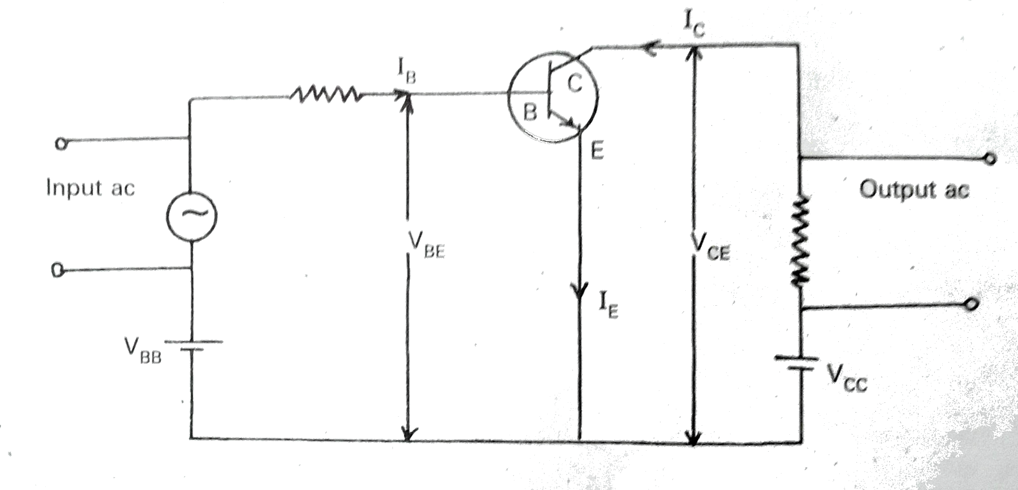
The n-p-n common emitter amplifier circuit is shown in figure. In this circuit the battery VBB provides the biasing voltage VBE for the base emitter junction. The emitter junction is forward biased and the battery VCC provides the biasing voltage VCE for the emitter collector junction.The junction is reverse biased . Most of the electron from emitter cross the base region and move into the collector.
The input signal to the amplified is connected in series with the biasing battery(VBB) .A load resistance RL is connected in the collector circuit and output voltage is taken across RL.
As the base emitter voltage(VBE) changes due to input signal, the base current changes (IB). This results in large change in collector current (ΔIC). The change in collector emitter voltage (ΔVCE) is taken across RL . Thus amplified output is obtained across RL.
Current gain (β) : The ratio of change in collector current to the change in base current is called current gain (or ) current amplification factor.
β=ΔICΔIB
Voltage gain (AV): It is the ratio of change in output voltage (ΔVCE)to the change in input voltage (ΔVBE).
Voltage gain =ΔVCEΔVBE=β×RLRi
Power gain : It is defined as the product of current gain and voltage gain.
Powergain (Ap)= Current gain × Voltage gain.
|
Topper's Solved these Questions
- SEMICONDUCTOR ELECTRONICS : MATERIALS , DEVICES , AND SIMPLE CIRCUITS BOOK - VIKRAM PUBLICATION ( ANDHRA PUBLICATION)CHAPTER - SEMICONDUCTOR ELECTRONICS : MATERIALS , DEVICES , AND SIMPLE CIRCUITS EXERCISE - TEXTUAL EXERCISES
11 Videos
- SEMICONDUCTOR ELECTRONICS : MATERIALS , DEVICES , AND SIMPLE CIRCUITS BOOK - VIKRAM PUBLICATION ( ANDHRA PUBLICATION)CHAPTER - SEMICONDUCTOR ELECTRONICS : MATERIALS , DEVICES , AND SIMPLE CIRCUITS EXERCISE - ADDITIONAL EXERCISES
8 Videos
- SEMICONDUCTOR ELECTRONICS : MATERIALS , DEVICES , AND SIMPLE CIRCUITS BOOK - VIKRAM PUBLICATION ( ANDHRA PUBLICATION)CHAPTER - SEMICONDUCTOR ELECTRONICS : MATERIALS , DEVICES , AND SIMPLE CIRCUITS EXERCISE - SHORT ANSWER QUESTIONS
16 Videos
- RAY OPTICAL AND INSTRUMENTSBOOK - VIKRAM PUBLICATION ( ANDHRA PUBLICATION)CHAPTER - RAY OPTICAL AND INSTRUMENTSEXERCISE - TEXTUAL EXERCISES
60 Videos
- TELANGANA MARCH-2019BOOK - VIKRAM PUBLICATION ( ANDHRA PUBLICATION)CHAPTER - TELANGANA MARCH-2019EXERCISE - SECTION -B
5 Videos
Similar Questions
Knowledge Check
in common emitter amplifier, the emitter base junction is
Aforward biasBreverse biasCinsulatorDnone of theseIn a common emitter amplifier the input signal is applied across
AAny whereBEmitter-collectorCCollector-baseDBase - emitterThe value of amplification factor (β) in common emitter configuration is
A=1B<1C≤1D>1
Draw the circuit diagram of a common emitter amplifier using n-p-n transistor. What is the phase difference between the input signal and output voltage? State two reasons why a common emitter amplifier is preferred to a common base amplifier.
View SolutionDraw a labelled circuit diagram of a transistor acting as a common emitter amplifier. What is meant by phase reversal?
View SolutionA transistor is used in a common emitter mode as an amplifier. Then
View SolutionIf a transistor is used in common -emitter mode as an amplifier,then
View SolutionA transistor is used in the common emitter mode as an amplifier . Then
View Solution
