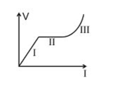
Transfer characterstics [output voltage (Vo) vs. input voltage (Vi)] for a base biased transistor in CE configuration is as shown in the figure. For using transfor as a which, it is used
![Transfer characterstics [output voltage (V(o)) vs. input voltage (V(i))] for a base biased transistor in CE configuration is as shown in the figure. For using transfor as a which, it is used](https://d10lpgp6xz60nq.cloudfront.net/physics_images/BMS_OBJ_XII_C13_E01_387_Q01.png)
in region I
in region III
both in regios (I) and in (III)
in region II
The correct Answer is:C
For using transistor as a switch, it is used in cut-off state
Topper's Solved these Questions
- BOOK - A2ZCHAPTER - SEMICONDUCTOR ELECTRONICSEXERCISE - AIIMS Questions38videos
SEMICONDUCTOR ELECTRONICS
- BOOK - A2ZCHAPTER - SEMICONDUCTOR ELECTRONICSEXERCISE - Assertion Reason18videos
SEMICONDUCTOR ELECTRONICS
- BOOK - A2ZCHAPTER - SEMICONDUCTOR ELECTRONICSEXERCISE - Section B - Assertion Reasoning22videos
SEMICONDUCTOR ELECTRONICS
- BOOK - A2ZCHAPTER - NUCLEAR PHYSICSEXERCISE - Section D - Chapter End Test29videos
NUCLEAR PHYSICS
- BOOK - A2ZCHAPTER - SOURCE AND EFFECT OF MAGNETIC FIELDEXERCISE - Section D - Chapter End Test30videos
SOURCE AND EFFECT OF MAGNETIC FIELD
Similar Questions
Knowledge Check
- Question 1 - Select One
An input voltage Vi of 0.20V is applied to an operational amplifier connected as shown in the diagram. What is the output voltage V0?
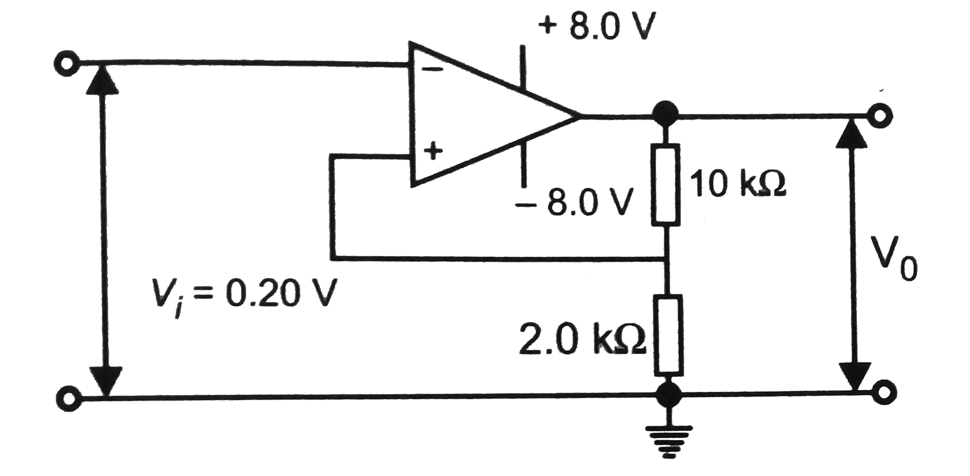 A0.20VB1.2VC0.80VD8.0V
 - Question 2 - Select One
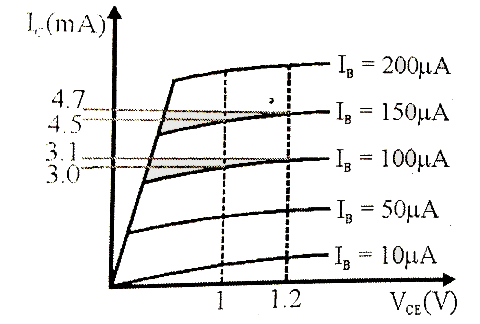
Output characteristic of n-p-n transistor in CE configuration is shown. From the characteristic curve determine the current gain at VCE=1V-A30B32C28D40 - Question 3 - Select One
In a voltage regulating of zener diode, the graph of output voltage vo versus input voltage v1 is
A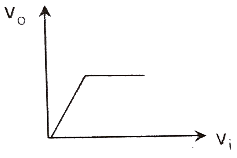 B
B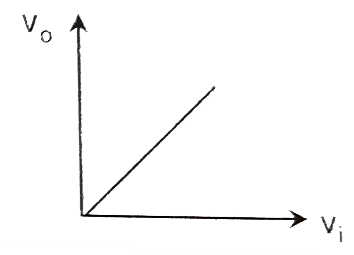 C
C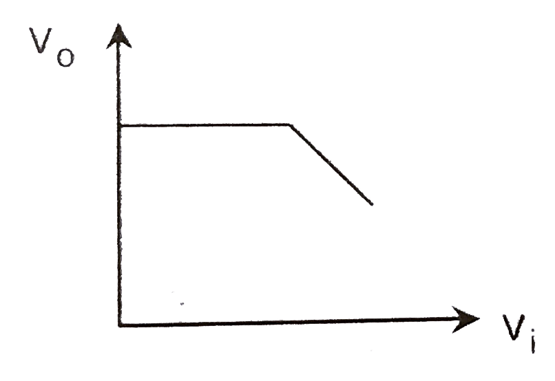 D
D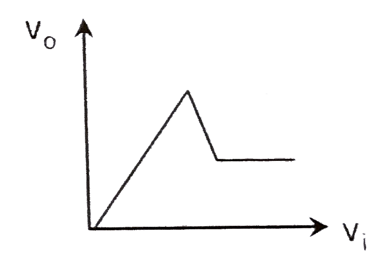
Draw the tramsfer characteristic curve of a base biased transistor in CE configuration. Explain clearly how the active region of the Vo versus Vi curve in a transistor is used as an amplifier.
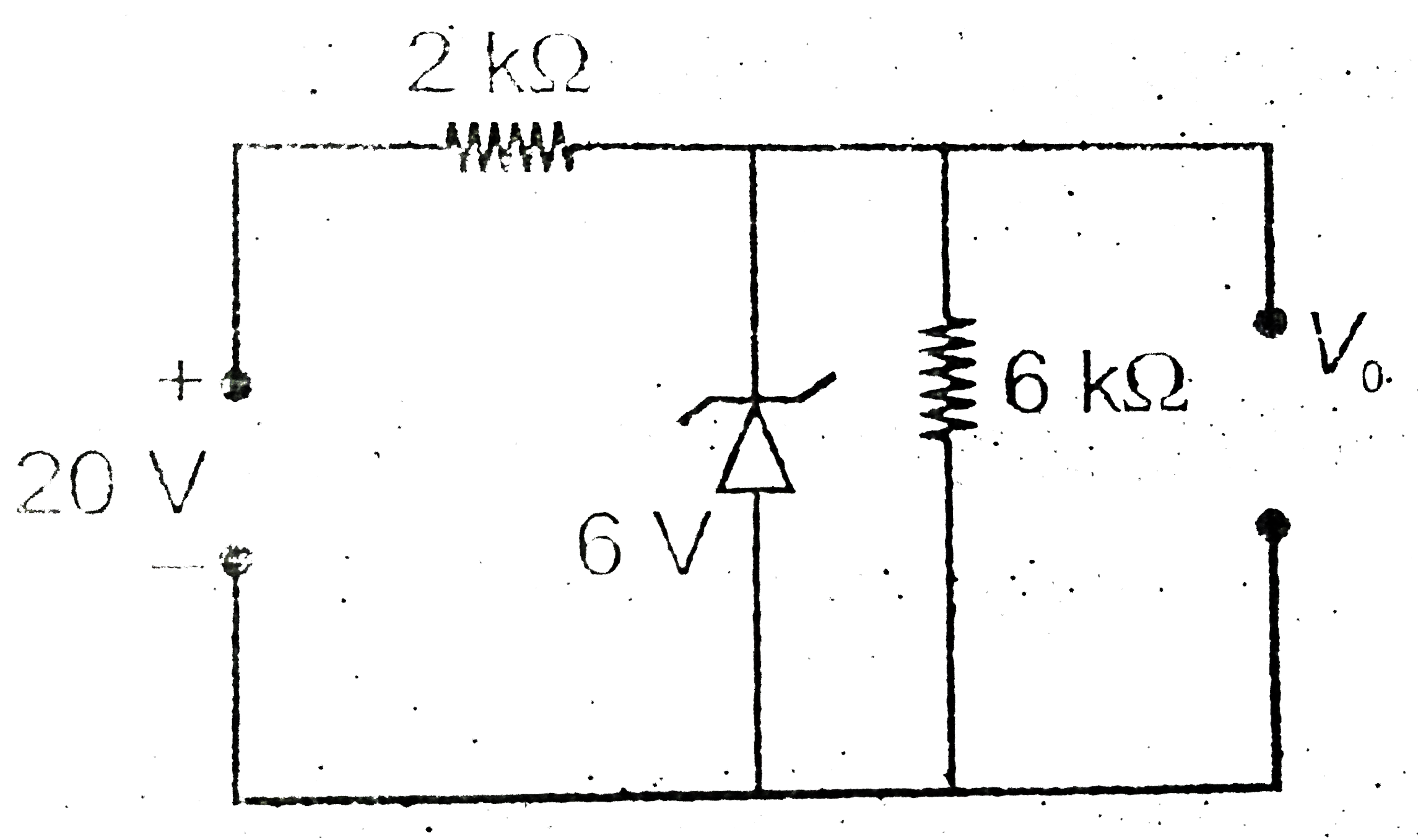
View SolutionWhat is the value of output voltage V0 in the circuit shown in the figure ?
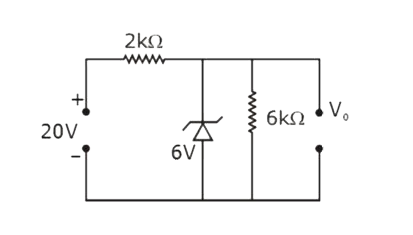 View Solution
What is the value of output voltage V0 in the circuit shown in the figure ?
 View Solution
What is the phase relationship in the output and input voltage in the common base transistor amplifier.
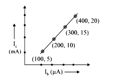
View SolutionThe transfer characteristic curve of a transistor, having input and output resistance 100Ωand100kΩ respectively, is shown in the figure. The Voltage and Power gain, are respectively:
 View Solution


