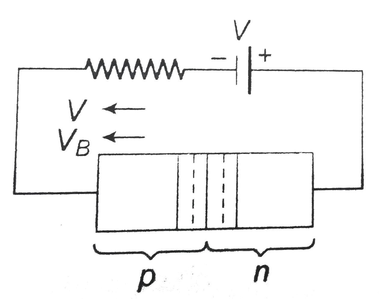
Reverse bias applied to a junction diode
no current flow
the depletion region is reduced
the height of the potential barrier is reduced
the depletion region is increased
The correct Answer is:D
In reverse biasing, the applied voltage V on the n-side is positive and is negative on the P -side. The applied biase V and the barrier potential VB are in the same direction making the effective junciton potential V+VB. As a result, the junction width will increases. the higher junction potential would restrict the flow of majority carriers to a much greater extent. However, such a field will favour the flow of minority carriers. So, reverse biase current will be due to the minority carriers only

Topper's Solved these Questions
- BOOK - A2ZCHAPTER - SEMICONDUCTOR ELECTRONICSEXERCISE - Assertion Reason18videos
SEMICONDUCTOR ELECTRONICS
- BOOK - A2ZCHAPTER - SEMICONDUCTOR ELECTRONICSEXERCISE - SECTION -D1videos
SEMICONDUCTOR ELECTRONICS
- BOOK - A2ZCHAPTER - SEMICONDUCTOR ELECTRONICSEXERCISE - AIPMT/NEET Questions77videos
SEMICONDUCTOR ELECTRONICS
- BOOK - A2ZCHAPTER - NUCLEAR PHYSICSEXERCISE - Section D - Chapter End Test29videos
NUCLEAR PHYSICS
- BOOK - A2ZCHAPTER - SOURCE AND EFFECT OF MAGNETIC FIELDEXERCISE - Section D - Chapter End Test30videos
SOURCE AND EFFECT OF MAGNETIC FIELD
Similar Questions
Knowledge Check
- Question 1 - Select One
The reverse biassing in a junction diode
Adecreases the potential barrierBincreases the potential barrierCincrease the number of majority charge carriersDnone of these - Question 2 - Select One
The reverse biasing in a PN junction diode
ADecreases the potential barrierBIncreases the potential barrierCIncreases the number of minority charge carriersDIncreases the number of majority charge carriers - Question 3 - Select One
The reverse biasing in a p-n junction diode
Adecreases the potential barrier.Bincreases the potential barrier.Cincreases the number of minority charge carriers.Dincreases the number of majority charge carriers.
The reverse bias in a junction diode is changed from 5V to 15V then the value of current changes from 38μA to 88μA. The resistance of junction diode will be.
View SolutionWhen a forward bias is applied to a p-n junction, it
View SolutionThe approximate ratio of resistance in the forward and reverse biase of the PN− junction diode is
View SolutionA Si and a Ge diode has identical physical dimensions. The band gap in Si is larger than that in Ge. An indentical reverse bias is applied across the diodes.
View SolutionNo bias is applied to a P-N junction, then the current-
View Solution

