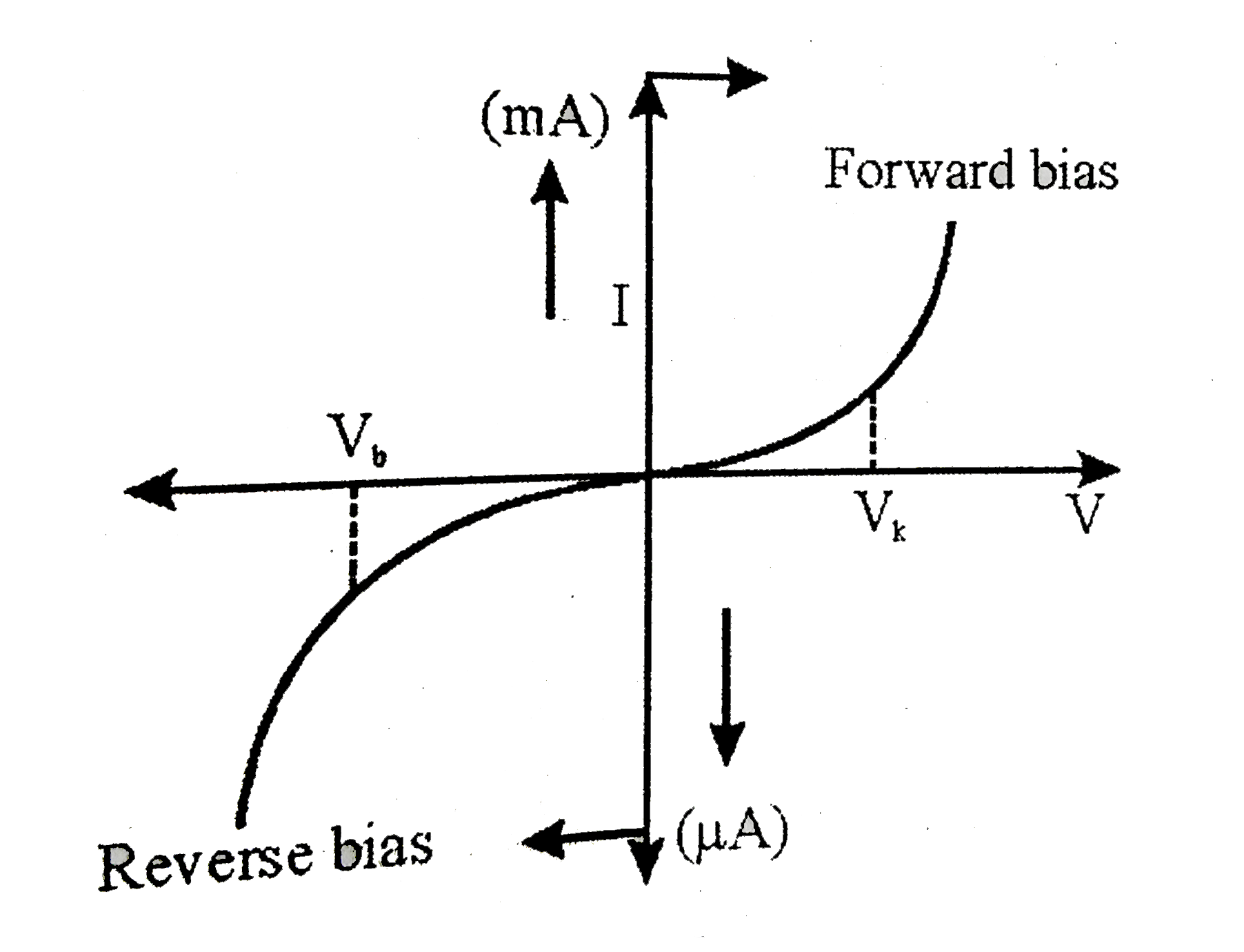
Draw V-I characterictics of a p-n junction diode. Why does the reverse current show a sudden increase at the critical voltage?
Name any semiconductor device which operates under the reverse bias in the breakdown region.
For V-I characteristics of a p-n junction, see Fig.and Fig.
When p-n junction is operated under a reverse bias condition a very small reverse current (about few muA) flows due to drifting of minirity charge carriers, which is independent of the applied potential upto a critical voltage.
When the reverse voltage across the p-n junction reaches a critical voltage, the reverse current suddenly rises to a large value. It is due to sudden increase in the number of minority charge carriers, resulting breakdown of the diode. If the p-n junction is lightly doped, the avalanche breakdown occurs due to ionisation by collosion. If the p-n junction is heavily doped, the zener breakdown occurs at even low oltages due to field emission.
Asemiconductor device which operates under the reverse bias in the breakdown region is the zener diode.
Topper's Solved these Questions
- BOOK - PRADEEPCHAPTER - ELECTRONIC DEVICESEXERCISE - SAMPLE PROBLEM2videos
ELECTRONIC DEVICES
- BOOK - PRADEEPCHAPTER - ELECTRONIC DEVICESEXERCISE - CONCEPTUAL PROBLEMS1videos
ELECTRONIC DEVICES
- BOOK - PRADEEPCHAPTER - ELECTROMAGNETIC WAVESEXERCISE - II Focus multiple choice question5videos
ELECTROMAGNETIC WAVES
- BOOK - PRADEEPCHAPTER - ELECTROSTATICSEXERCISE - ASSERTION-REASON TYPE QUESTIONS2videos
ELECTROSTATICS
Similar Questions
Draw V-I characteristicsof a p-n junction diode. Answer the following questions, giving reasons:
(i) Why is the current under reverse bias almost independent of the applied potential upto a critical voltage ?
(ii) Why does the reverse current show a sudden increase at the critical voltage ? Name any semiconductor device which operates under the reverse bias in the breakdown region.View SolutionDraw the V-I characterisitics of p-n junction diode in forward bias and in reverse bias.
View Solution
Knowledge Check
- Question 1 - Select One
On increasing reverse voltage in a p−n junction diode the value of reverse current will
Agradually increasesBfirst remains constant and then suddenly increaseCremains constantDgradually decrease - Question 2 - Select One
In the case of a p-n junction diode, if the reverse bias is very high, there is a sudden large increase in current. In this case the value of reverse bias voltage is known as
ACutoff voltageBCritical voltageCKnee voltageDZener voltage - Question 3 - Select One

The V-I characterisctic for a p-n junction diode is plotted as shown in the figure. From the plot we can conclude that
[Vb→ breakdown voltage, Vk→ knee voltage]Athe forward bias resistance of diode is very high, almost infinity for small values of V and after a certain value it becomes very lowBthe reverse bias resistance of diode is very high in the beginning upto breakdown voltage is not achievedCboth forward and reverse bias resistances are same for all voltagesDboth (A) and (B) are correct
In V-I characteristics of a p-n junction diode, why is the current under reverse bias almost independence of the applied potential upto a critical voltage?
View SolutionIn a p-n junction diode the reverse saturation current is 10μA. What will be the forward current for a voltager of 0.2 V ?
View Solution(a). Explains briefly with the help of a circuit diagram how V-I characteristics of a p-n junction diode are obtainedin (i) forward bias, and (ii) reverse bias.
(b). A photo diode is fabricated from a semiconductor with a band gap of 2.8 EV. Can it detect wave length of 6000. nm? Justify.View SolutionHow does the width of the depletion layer of a p-n junction diode change with decrease in reverse bias?
View Solution(a) Draw the V-I characteristic curve for forward and reverse bias of a p-n juction diode
(b) what are th majority and ninority carriers in a p type semiconductor
(c ) wirte down the symbol and truth table of OR gateView Solution

