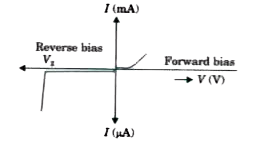
(a) Draw the V-I characteristic curve for forward and reverse bias of a p-n juction diode
(b) what are th majority and ninority carriers in a p type semiconductor
(c ) wirte down the symbol and truth table of OR gate
Step by step video & image solution for (a) Draw the V-I characteristic curve for forward and reverse bias of a p-n juction diode (b) what are th majority and ninority carriers in a p type semiconductor (c ) wirte down the symbol and truth table of OR gate by Physics experts to help you in doubts & scoring excellent marks in Class 12 exams.
Updated on:21/07/2023Topper's Solved these Questions
- SEMICONDUCTOR ELECTRONICS METERIALS DEVICES AND SIMPLE CIRCUITS BOOK - MODERN PUBLICATIONCHAPTER - SEMICONDUCTOR ELECTRONICS METERIALS DEVICES AND SIMPLE CIRCUITS EXERCISE - REVISION EXERCISES( LONG ANSWER QUESTIONS)
11 Videos
- SEMICONDUCTOR ELECTRONICS METERIALS DEVICES AND SIMPLE CIRCUITS BOOK - MODERN PUBLICATIONCHAPTER - SEMICONDUCTOR ELECTRONICS METERIALS DEVICES AND SIMPLE CIRCUITS EXERCISE - REVISION EXERCISES (NUMERICAL PROBLEMS )
15 Videos
- SEMICONDUCTOR ELECTRONICS METERIALS DEVICES AND SIMPLE CIRCUITS BOOK - MODERN PUBLICATIONCHAPTER - SEMICONDUCTOR ELECTRONICS METERIALS DEVICES AND SIMPLE CIRCUITS EXERCISE - REVISION EXERCISES(FILL IN THE BLANKS )
10 Videos
- RAY OPTICS AND OPTICAL INSTRUMENTSBOOK - MODERN PUBLICATIONCHAPTER - RAY OPTICS AND OPTICAL INSTRUMENTSEXERCISE - CHAPTER PRACTICE TEST
14 Videos
- WAVE OPTICALBOOK - MODERN PUBLICATIONCHAPTER - WAVE OPTICALEXERCISE - CHAPTER PRACTICE TEST
7 Videos
Similar Questions
Knowledge Check
What accounts for the flow of charge carriers in forward and reverse biasing of sillicon P-N diode-
Adrift in both reverse and forward biasBdrift in forward bias and diffusion in reverse biasCdrift in reverse bias and diffusion in forward biasDdiffution in both forward and reverse biasWhen forward bias is applied to a P−N junction, then what happence to the potential barrier VB, and the width of charge depleted region x?
AVB increase, x decreasesBVB decreases, x increasesCVB increase, x increasesDVB decrease, x decreases
Draw V-I characterictics of a p-n junction diode. Why does the reverse current show a sudden increase at the critical voltage?
Name any semiconductor device which operates under the reverse bias in the breakdown region.
View Solution(a). Explains briefly with the help of a circuit diagram how V-I characteristics of a p-n junction diode are obtainedin (i) forward bias, and (ii) reverse bias.
(b). A photo diode is fabricated from a semiconductor with a band gap of 2.8 EV. Can it detect wave length of 6000. nm? Justify.
View Solution

(a) Draw the circuit diagram of reversed bias p-n junction.
(b). Draw the output wavefrom across diode in given circuit.
(c). Draw the truth table for the given logic gate.
View SolutionExplain briefly, with the help of circuit diagram , how V-I characteristics of a p-n junction diode are obtained in (i) forward bias, and (ii) reverse bias. Draw the shapes of the characteristic curves obtained.
Or
Explain briefly, with the help of necessary diagrams, the forward and the reverse biasing of a p-n junction diode. Also draw their characteristic curves in the two cases.
View SolutionIn V-I characteristics of a p-n junction diode, why is the current under reverse bias almost independence of the applied potential upto a critical voltage?
View SolutionThe figure shows the V-I characteristic of a semiconductor diode designed to operate under revese bias

(a) identify the semiconductor diode used
(b) draw the cirucuit diagram to obtain the given characteristics of this devics
(c ) briefly expain one use of this device
View Solution
