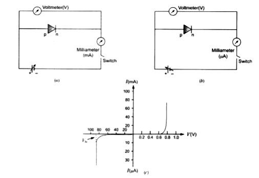
Using the necessary circuit diagram, show how the V-I characteristics of a p-n junction are obtained in (i) forward biasing (ii) Reverse biasing. How are these characteristics made use of in rectification?
The circuit arrangement for studying the V–l characteristics of a diode are shown in Fig. (a) and (b). For different values of voltages the value of current is noted. A graph between V and is obtained as in Figure (c).
From the V-l characteristic of a junction diode it is clear that it allows current to pass only when it is forward biased. So if an alternating voltage is applied across a diode the current flows only in that part of the cycle when the diode is forward biased. This property is used to rectify alternating voltages.

Topper's Solved these Questions
- CBSE Examination Paper Delhi–2014BOOK - CBSE COMPLEMENTARY MATERIALCHAPTER - CBSE Examination Paper Delhi–2014EXERCISE - Set-II (Questions Uncommon to Set-I)
10 Videos
- CBSE Examination Paper Delhi–2014BOOK - CBSE COMPLEMENTARY MATERIALCHAPTER - CBSE Examination Paper Delhi–2014EXERCISE - SET-III (Questions Uncommon to set-I and II)
9 Videos
- CBSE EXAMINATION PAPER - 2016 BOOK - CBSE COMPLEMENTARY MATERIALCHAPTER - CBSE EXAMINATION PAPER - 2016 EXERCISE - SECTION - E
17 Videos
- CBSE EXAMINATION PAPER, DELHI REGION - 2015 (CODE NO. 55/1/1/D)BOOK - CBSE COMPLEMENTARY MATERIALCHAPTER - CBSE EXAMINATION PAPER, DELHI REGION - 2015 (CODE NO. 55/1/1/D)EXERCISE - SECTION E
6 Videos
Similar Questions
Using the necessary circuit diagram, show how the V-I characteristics of a p-n junction are obtained in (i) forward biasing (ii) Reverse biasing. How are these characteristics made use of in rectification?
View SolutionUsing the necessary circuit diagrams, show how the V-I characteristics of a p-n junction are obtained in
(i) Forward baising
(ii) Reverse biasing.
View Solution
Knowledge Check
In V- I characteristics of p−n junction in reverse biasing results in
Aleakeage currentBthe current which cannot be neglectedCno flow of currentDlarge current
(a) state briefly the processes involved in the formation of p-n how the depletion region is formed
(b) using the necessary circuit diagrams show p-n junction are obtained in
(i) forward biasing (ii) reverse biasing how these characteristic are made use of in rectification
View SolutionExplain briefly, with the help of circuit diagram , how V-I characteristics of a p-n junction diode are obtained in (i) forward bias, and (ii) reverse bias. Draw the shapes of the characteristic curves obtained.
Or
Explain briefly, with the help of necessary diagrams, the forward and the reverse biasing of a p-n junction diode. Also draw their characteristic curves in the two cases.
View SolutionDraw the V-I characterisitics of p-n junction diode in forward bias and in reverse bias.
View Solution(a). Explains briefly with the help of a circuit diagram how V-I characteristics of a p-n junction diode are obtainedin (i) forward bias, and (ii) reverse bias.
(b). A photo diode is fabricated from a semiconductor with a band gap of 2.8 EV. Can it detect wave length of 6000. nm? Justify.
View SolutionP-N junction biasing and characteristics
View SolutionWhat happens to the width of depletion layer of a p-n junction when it is (i) forward biased, (ii) reverse biased?
View SolutionWhat is the deffect on current when a p-n diode is (i) forward biased (ii) reverse biased
View Solution
