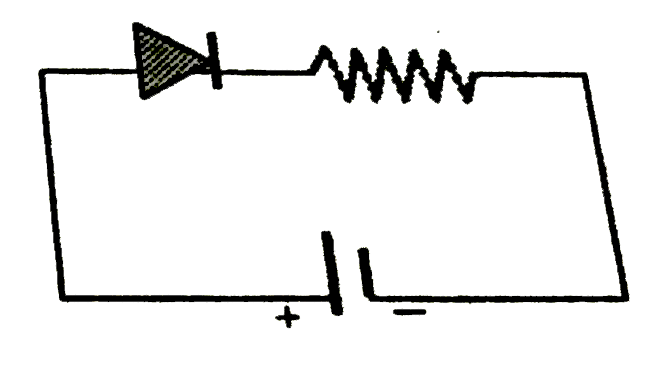
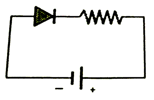
Give three differences between forward bias and reverse bias.
Step-by-Step Solution
1. Definition of Forward Bias and Reverse Bias:
- Forward Bias: In forward bias, the positive terminal of the battery is connected to the p-type material and the negative terminal is connected to the n-type material of a diode. This allows current to flow through the diode.
- Reverse Bias: In reverse bias, the positive terminal of the battery is connected to the n-type material and the negative terminal is connected to the p-type material. This prevents current from flowing through the diode.
2. Current Flow:
- Forward Bias: The current flow is primarily due to the majority charge carriers. In the case of a p-n junction diode, the majority carriers are holes in the p-type material and electrons in the n-type material.
- Reverse Bias: The current flow is primarily due to minority charge carriers. In a p-n junction, the minority carriers are electrons in the p-type material and holes in the n-type material.
3. Magnitude of Current:
- Forward Bias: The current in forward bias is typically in the range of milliamperes (mA), which is 10^-3 amperes.
- Reverse Bias: The current in reverse bias is much smaller, usually in the microamperes (µA) range, which is 10^-6 amperes.
4. Depletion Layer Width:
- Forward Bias: The depletion layer width decreases when the diode is forward biased, allowing more charge carriers to flow through.
- Reverse Bias: The depletion layer width increases when the diode is reverse biased, which restricts the flow of charge carriers.
Summary of Differences
1. Current Flow:
- Forward Bias: Current flows due to majority charge carriers.
- Reverse Bias: Current flows due to minority charge carriers.
2. Magnitude of Current:
- Forward Bias: Current is in the range of milliamperes (mA).
- Reverse Bias: Current is in the range of microamperes (µA).
3. Depletion Layer Width:
- Forward Bias: Depletion layer decreases.
- Reverse Bias: Depletion layer increases.
- Forward Bias: In forward bias, the positive terminal of the battery is connected to the p-type material and the negative terminal is connected to the n-type material of a diode. This allows current to flow through the diode.
- Reverse Bias: In reverse bias, the positive terminal of the battery is connected to the n-type material and the negative terminal is connected to the p-type material. This prevents current from flowing through the diode.
- Forward Bias: The current flow is primarily due to the majority charge carriers. In the case of a p-n junction diode, the majority carriers are holes in the p-type material and electrons in the n-type material.
- Reverse Bias: The current flow is primarily due to minority charge carriers. In a p-n junction, the minority carriers are electrons in the p-type material and holes in the n-type material.
- Forward Bias: The current in forward bias is typically in the range of milliamperes (mA), which is 10^-3 amperes.
- Reverse Bias: The current in reverse bias is much smaller, usually in the microamperes (µA) range, which is 10^-6 amperes.
- Forward Bias: The depletion layer width decreases when the diode is forward biased, allowing more charge carriers to flow through.
- Reverse Bias: The depletion layer width increases when the diode is reverse biased, which restricts the flow of charge carriers.
1. Current Flow:
- Forward Bias: Current flows due to majority charge carriers.
- Reverse Bias: Current flows due to minority charge carriers.
- Forward Bias: Current is in the range of milliamperes (mA).
- Reverse Bias: Current is in the range of microamperes (µA).
- Forward Bias: Depletion layer decreases.
- Reverse Bias: Depletion layer increases.
Topper's Solved these Questions
- ELECTRONIC DEVICES BOOK - CBSE COMPLEMENTARY MATERIALCHAPTER - ELECTRONIC DEVICES EXERCISE - LONG ANSWER QUESTIONS (5 MARKS)
1 Videos
- ELECTRONIC DEVICES BOOK - CBSE COMPLEMENTARY MATERIALCHAPTER - ELECTRONIC DEVICES EXERCISE - NUMERICALS
7 Videos
- ELECTRONIC DEVICES BOOK - CBSE COMPLEMENTARY MATERIALCHAPTER - ELECTRONIC DEVICES EXERCISE - SHORT ANSWER QUESTIONS (2 MARKS)
13 Videos
- ELECTROMAGNETIC WAVES AND OPTICSBOOK - CBSE COMPLEMENTARY MATERIALCHAPTER - ELECTROMAGNETIC WAVES AND OPTICSEXERCISE - 1 mark question
11 Videos
- ELECTROSTATICS AND CURRENT ELECTRICITY BOOK - CBSE COMPLEMENTARY MATERIALCHAPTER - ELECTROSTATICS AND CURRENT ELECTRICITY EXERCISE - NUMERICALS
49 Videos
Similar Questions
The V-I characteristics of silicon diode is shown in Fig. Calculate the diode resistance in forward bias at V=+0.9V reverse bias V=−3.0V.
View Solution(a). Explains briefly with the help of a circuit diagram how V-I characteristics of a p-n junction diode are obtainedin (i) forward bias, and (ii) reverse bias.
(b). A photo diode is fabricated from a semiconductor with a band gap of 2.8 EV. Can it detect wave length of 6000. nm? Justify.
View Solution
Knowledge Check
Which one is in forward bias
A B
B C
C DNone of these
A Zener diode when used as a voltage regulator is connected
(a) in forward bias
(b) in reverse bias
( c) in parallel to the load
(d) in series to the load.A(a) and (b) are correctB(b) and ( c) are correctC(a) only is correctD(d) only is correctA Zener diode when used as a voltage regulator is connected
(a) in forward bias
(b) in reverse bias
( c) in parallel to the load
(d) in series to the load.A(i) and (ii) are correctB(ii) and (iii) are correctC(i) only correctD(iv) only correct
A 3V battery may be connected across the point A and B as shown in Fig. Assume that the resistance of each diode is zero in the forward bias and infinity in the reverse bias. Find the current supplied by the battery if the positive terminal of the battery is connected to the point A the point B.
View SolutionDraw the V-I characterisitics of p-n junction diode in forward bias and in reverse bias.
View SolutionA p-n junction offers a high resistance in forward bias and a low resistance is reverse bias.
View SolutionAssertion : The dominant mechanism for motion of charge carreis in forward and reverse biased silicon P-N junction are drit in both forward and reverse bias.
Reaon : In reverse biasing, no current flow through the junction.
View SolutionGender bias refers to
View Solution
