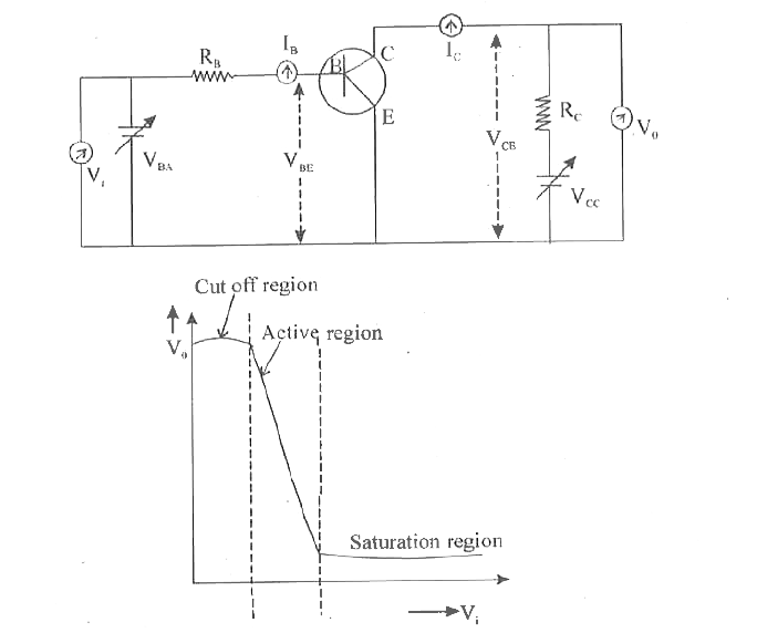
With a neat circuit diagram, explain the working of an npn transistor in CE node as a switch .
Text Solution

A device which turns on or off the electric current in an electric circuit is known as switch . The behaviour of the base biased transistor in CE - configuration is shown in the figure .
Applying Kirchhoff.s voltage law,
VBA=IBRB+VBE
and VCC=ICRC+VCE
VCE=VCC−ICRC
We shall assume VBB as the dc input and VCE as the dc output.
i.e., Vi−IBRB+VBE...(1)
Vo=VCC−RCIC...(2)
Vo changes when Vi increases from zero upwards.
Case (i): When Vi a 0.6 V1 there is no collector current , and the transistor will be in the cut off region.
VO=VCC
Case (ii): When Vi is between 0.6 to 1.0 V , the collector current IC increases and VO is decreases due to increase in ICRC and the transistor is in the active region.
Case (iii) : When Vi≤1.0 V , the transistor will have maximum possible collector current IC i.e., ICRC will be maximum and VO will tend to wands zero but will never become zero and the transistor is in saturation state.
From the above, we note that as long as Vi is low , VO is high and IC is nearly equal to zero. Under this condition the transistor is not working . It is said to be in switch of state. If Vi is high , VO is low and IC is maximum , and the transistor is said to be in switch on state. We can say that low input switches the transistor off and a high input . Switches it on. This indicates that a transistor acts as a switch.
|
Topper's Solved these Questions
Similar Questions
Knowledge Check
Transistors can work as a switch in
Abiasing regionBcut off regionCdepletion regionDnone of these
Transistors can work as a switch in
View SolutionWith the help of a neat circuit diagram, explain the working of a photodiode. State its any'two uses.
View SolutionWith a neat labelled diagram, explain the working of a refracting telescope.
View SolutionWith a neat labelled diagram, explain the actionn of npn transistor in common base configuration
View SolutionWith a neat labelled energy band diagram, explain the working of an LED.
View SolutionExplain, how a CE transistor acts as a switch.
View SolutionExplain the working of transistor as an oscillator using a labelled circuit diagram.
View Solution
