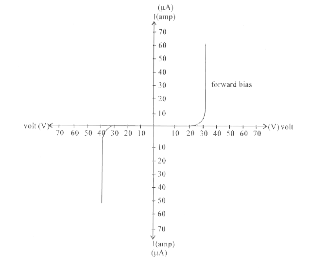
Explain the working of a semiconductor diode when it is forward biased. Draw the I-V characteristics for both forward bias and reverse bias of a semiconductor diode. Solution in Kannada

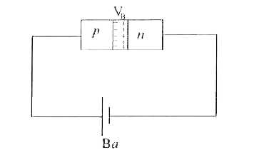
When the +ve terminal of a battery is connected to the p region and the -ve terminal battery is connected to the n-region of the junction diode , then the p-n junction is said to be forward biased.
When a battery is connected across the p-n junction diode , a p.d of .v. volt is applied across the diode . The resistance of depletion region is very high as it has no free charge carriers.As a result of this , the potential barrier height is reduced and width of deplection layer is decreased.
The +ve potential of the p-region attracts the electrons from the n-regions and the -ve potential of the n-region attracts the holes from the p-region. Due to these , the diffusion of majority carriers takes place across the junction . Thus an electric current will flow due to migration of majority carriers across the p-n junction, which is called forward current.

Topper's Solved these Questions
Similar Questions
Derive an expression for electrical conductivity.
View SolutionObtain an expression for the force between two straight parallel conductor carrying current. Hence define ampere.
View SolutionThe V-I characteristics of silicon diode is shown in Fig. Calculate the diode resistance in forward bias at V=+0.9V reverse bias V=-3.0V .
View SolutionThe V-I characteristic of a diode is shown in the figure. The ratio of forward to reverse bias resistance is
View SolutionDraw and explain the current -voltage (I-V) characteristic curves of a junction diode in forward and reverse bias.
View SolutionDraw the V-I characterisitics of p-n junction diode in forward bias and in reverse bias.
View SolutionExplain the working of a forward biased p-n junction diode.
View SolutionDraw the circuit arrangement for studying the V - I characteristics of a p-n junction diode in (i) forward and (ii) reverse bias. Briefly explain how the typical V - I characteristics of a diode are obtained and draw these characteristics.
View SolutionSemiconductor Diode|Forward Bias and Reverse Bias
View SolutionThe V-I characteristic of a diode is shown in the figure. The ratio of forward to reverse bias resistance is
View SolutionExplain forward bias and reverse bias of the junction diode.
View SolutionWhat is junction diode ? How is depletion layer formed ? Draw its forward and reverse bias characteristics by showing biasing of diodes ?
View Solutionअग्रसित बायस वाला डायोड़ जोड़ है :
View SolutionDraw the experimental circuit arrangement for studying V-I characteristics of a p-n junction diode in forward and reverse bias.
View SolutionDraw the V~I characteristic curves of a semiconductor diode for forward and reversed bias.
View Solution