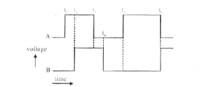
The wave forms A and B given below are given as input to a NAND gate . Then its logic output y is
 Solution in Tamil
for t1 to t2 , y = 0
for t2 to t3 , y = 1
for t3 to t4 , y = 1
for t4 to t5 , y 0
The correct Answer is:C
Step by step video, text & image solution for The wave forms A and B given below are given as input to a NAND gate . Then its logic output y is by Physics experts to help you in doubts & scoring excellent marks in Class 12 exams.
Topper's Solved these Questions
- BOOK - NEW JOYTHI PUBLICATIONCHAPTER - SEMICONDUCTOR ELECTRONICS : MATERIALS , DEVICES AND SIMPLE CIRCUITS EXERCISE - PREVIOUS YEAR QUESTIONS3videos
SEMICONDUCTOR ELECTRONICS : MATERIALS , DEVICES AND SIMPLE CIRCUITS
- BOOK - NEW JOYTHI PUBLICATIONCHAPTER - RAY OPTICS AND OPTICAL INSTRUMENTS EXERCISE - COMPETITIVE EXAM CORNER26videos
RAY OPTICS AND OPTICAL INSTRUMENTS
- BOOK - NEW JOYTHI PUBLICATIONCHAPTER - WAVE OPTICSEXERCISE - COMPETITIVE EXAM CORNER17videos
WAVE OPTICS
Similar Questions
We are familiar with the semi conductors Silicon and Germanium .
a. With a necessary schematic diagram , briefly explain the characteristics of an intrinsic semiconductor.
b. Draw the energy bands of a n-type semiconductor.
c The following figure represents a
d . Draw a typically illuminated P-n junctions solar cell.
e. LED convert............ energy to light.03:38View SolutionA 100 W bulb produces an electric field of 2.9 V/m at a point 3m away. If the bulb is replaced by 400 W bulb without disturbing other conditions. Then the electric field produced at the same point is
04:20View SolutionYoung's experiment is performed with light of wavelength 6000Å where in 16 frignes occupy a certain region on the screen. If 24 fringes occupy the same region with another light of wavelength λ then λ is
04:08View SolutionSketch the output Y from NAND gate having input A A and B given below, Fig.
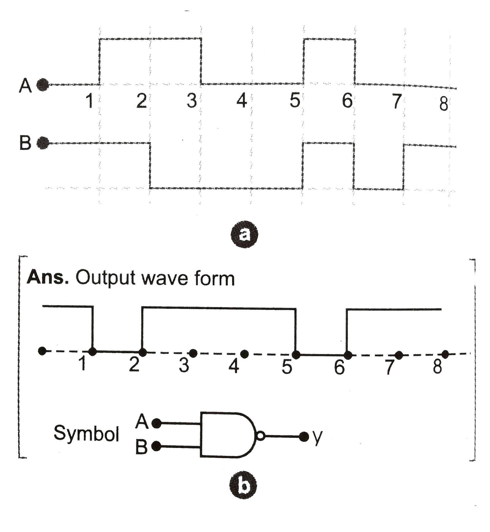
04:29View SolutionTwo signal A and B shown in the Fig. are used as two inputs of a NAND gate. Draw its output wave form. Give the logic symbol of NAND gate.
 04:29View Solution
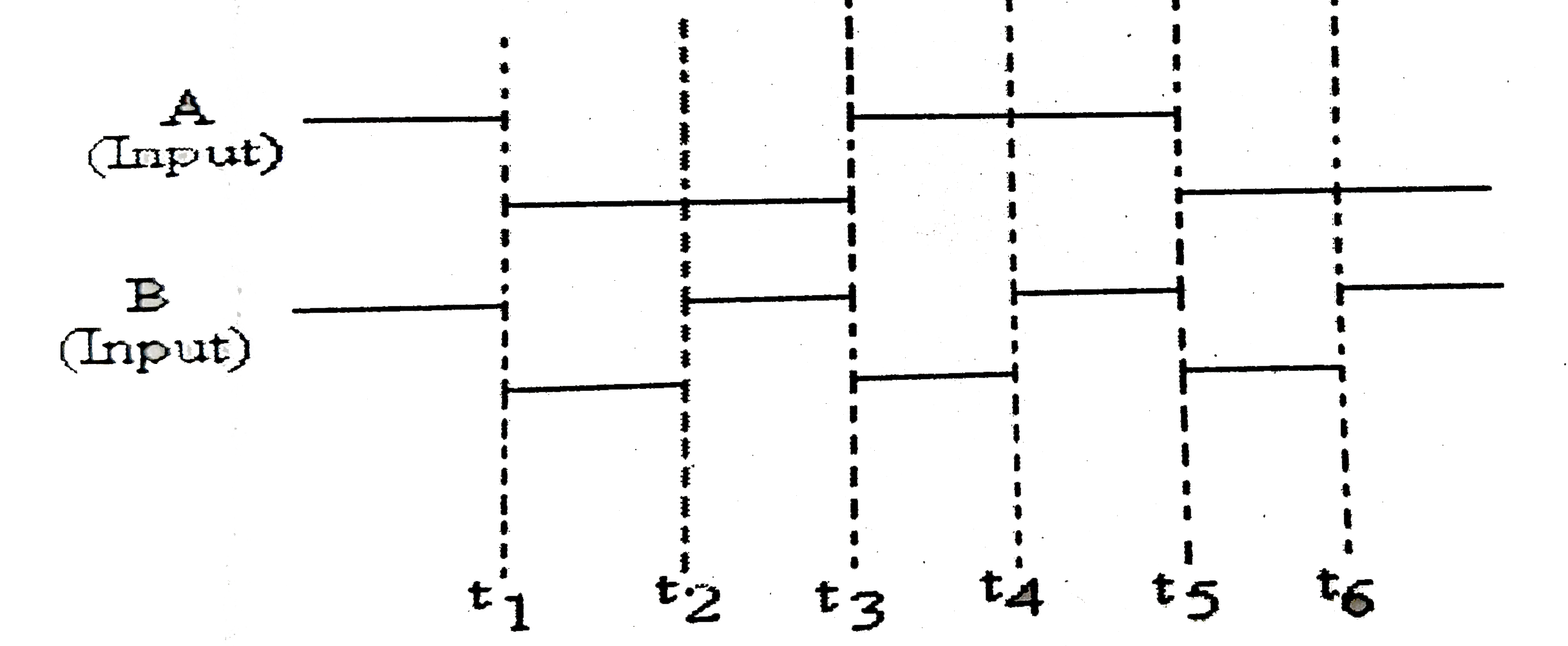
The give inputs A, B are fed to a 2-input NAND gate. Draw the output wave form of the gate.View Solutionनीचे दिखाए गए निवेश A तथा B के लिये NAND गेट के निर्गत तरंग रूप को स्केच कीजिए :
 03:27View Solution
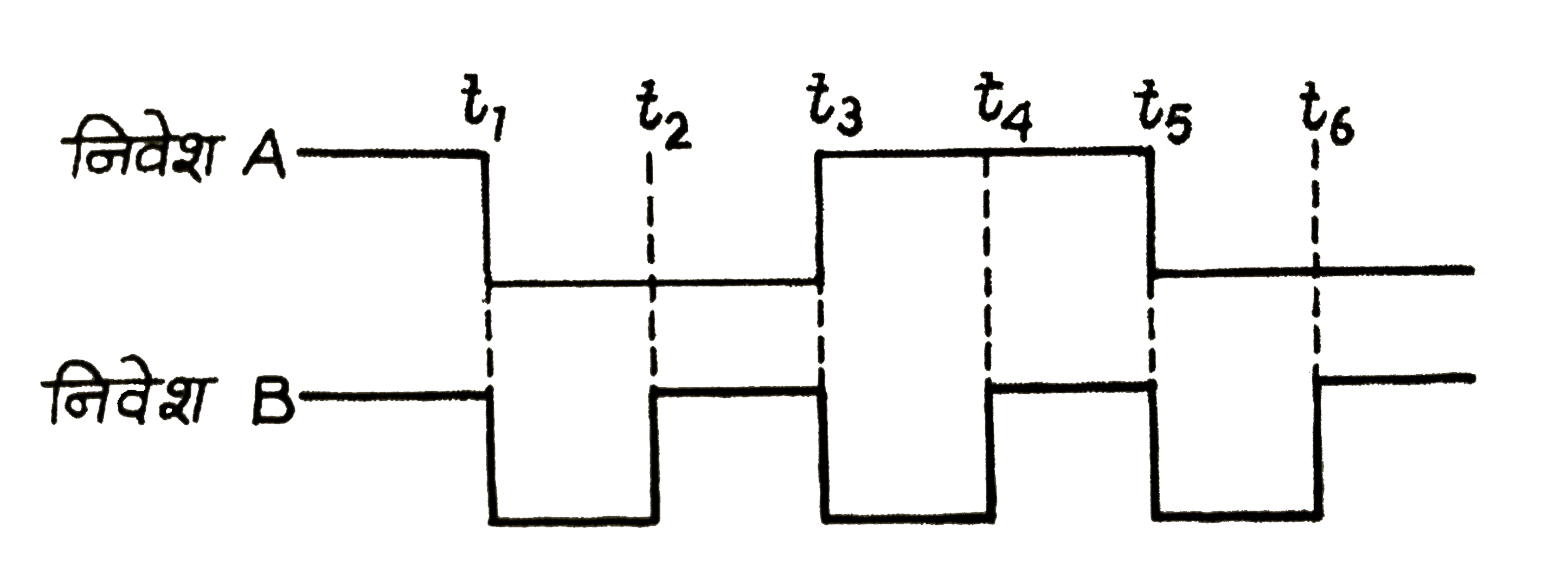
नीचे दिखाए गए निवेश A तथा B के लिये NAND गेट के निर्गत तरंग रूप को स्केच कीजिए :
 05:26View Solution
Sketch the output Y from a NAND gate having inputs A and B given below :
06:55View SolutionIf the Output of two NAND gates is given to input of a NAND gate. Then the truth table will be of
View SolutionSketch inputs A,B and output Y from a NAND gate from the table given below
View SolutionSketch the output Y from a NAND gate having inputs A and B given below .
06:24View SolutionSketch the output Y from a NAND gate having inputs A and B given below:
03:47View SolutionSketch the output Y from a NAND gate having inputs A and B given below:
04:01View SolutionSketch the output Y from a NAND gate having inputs A and B given below:
03:44View Solution

