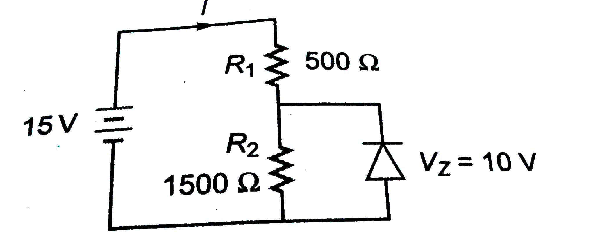
Give reason to explain why n and p regions of a Zener diode are heavily doped. Find the current through the Zener diode in the circuit given below (Zener breakdown voltage is 15 V).

Text Solution
Zener diode is fabricated by heavily doping bothp- and n sides of the p-n junction. As a result, the depletion region formed is very thin, even less than 106 m, and consequently the electric field at the junction is extremely high (of the order of 5×10⁶ V/m or even more) even for a small reverse bias voltage of about 5V and breakdown voltage has a low value of about 5V.
As per given circuit arrangement input voltage Vi = 20 V and voltage drop across zener diode (i.e., the zener breakdown voltage) = 15 V. Thus, voltage drop across series resistance of Rs = 250 , VR= 20-15 = 5 V.
∴ Current flowing through RS,I=VRR=5V250Ω=0.02A or 20 mA
As load resistance RL=1kΩ=1000Ω and voltage across RL = zener breakdown voltage VL = 15 V
∴ Current passing through load, IL=VLRL=15V1000Ω=0.015A=15 mA
Since zener diode and load are in parallel , hence zener current
IZ=I−IL=20 mA - 15 ma = 5 mA
|
Topper's Solved these Questions
- SEMICONDUCTOR ELECTRONICS : MATERIALS, DEVICES AND SIMPLE CIRCUITSBOOK - U-LIKE SERIESCHAPTER - SEMICONDUCTOR ELECTRONICS : MATERIALS, DEVICES AND SIMPLE CIRCUITSEXERCISE - LONG ANSWER QUESTIONS-I
22 Videos
- SEMICONDUCTOR ELECTRONICS : MATERIALS, DEVICES AND SIMPLE CIRCUITSBOOK - U-LIKE SERIESCHAPTER - SEMICONDUCTOR ELECTRONICS : MATERIALS, DEVICES AND SIMPLE CIRCUITSEXERCISE - SELF ASSESSMENT TEST (MULTIPE CHOICE QUESTIONS )SECTION A
3 Videos
- SEMICONDUCTOR ELECTRONICS : MATERIALS, DEVICES AND SIMPLE CIRCUITSBOOK - U-LIKE SERIESCHAPTER - SEMICONDUCTOR ELECTRONICS : MATERIALS, DEVICES AND SIMPLE CIRCUITSEXERCISE - VERY SHORT ANSWER QUESTIONS
33 Videos
- RAY OPTICS AND OPTICAL INSTRUMENTSBOOK - U-LIKE SERIESCHAPTER - RAY OPTICS AND OPTICAL INSTRUMENTSEXERCISE - SELF ASSESSMENT TEST (SECTION B)
3 Videos
- WAVE OPTICSBOOK - U-LIKE SERIESCHAPTER - WAVE OPTICSEXERCISE - SELF ASSESSMENT TEST SECTION C (VERY SHORT ANSWER QUESTIONS)
4 Videos
Similar Questions
Knowledge Check
In the given circuit the current through the zener diode is
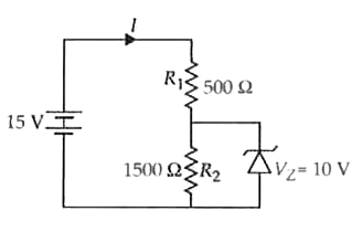 A10 mAB6.67 mAC5 mAD3.33 mA
In the circuit given, the current through the Zener diode is
 A10 mAB6.67 mAC5 mAD3.33 mA
In the circuit, Fig The current through the zener diode is
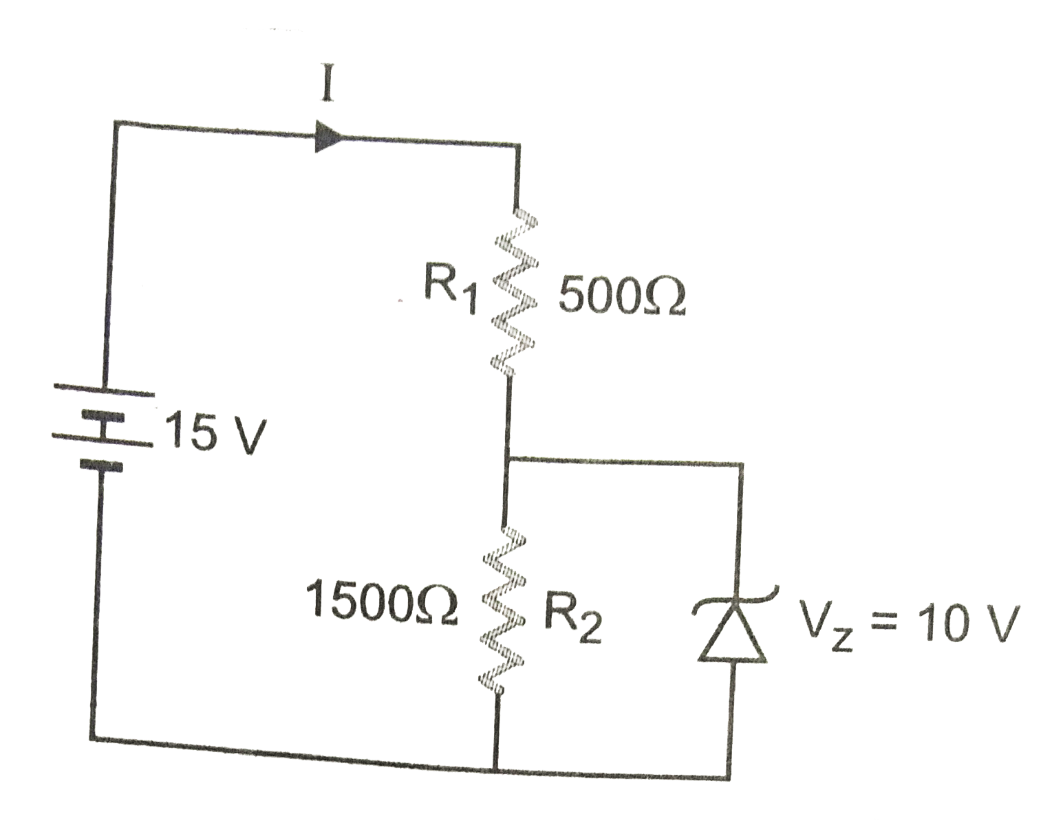 A10 mAB6.67 mAC5 mAD3.33 mA
In the circuit shown,find the current through the Zener diode.
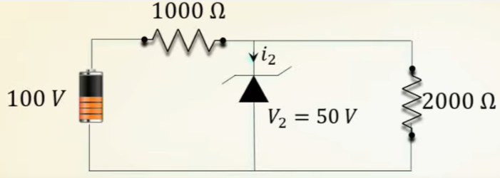
View SolutionIn the circuit, Fig.he current through the zener diode is

View SolutionFrom the Zener diode circuit shown in figure, the current through the Zener diode is
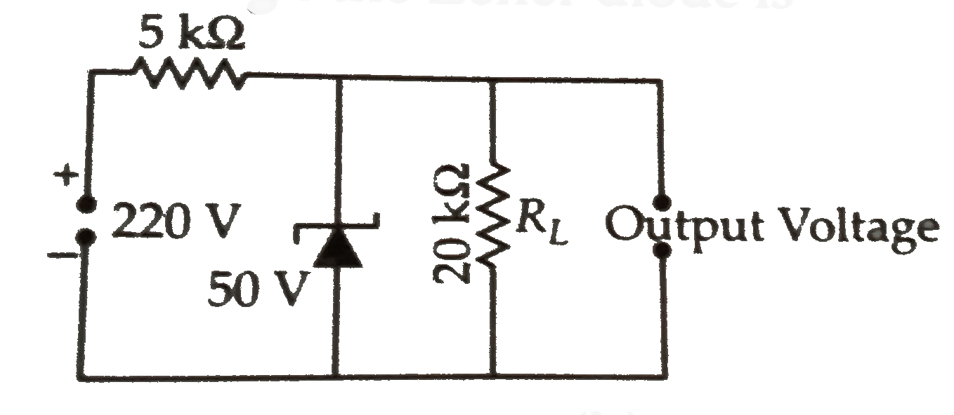
View SolutionFrom the Zener diode circuit shown in figure, the current through the Zener diode is

View SolutionFrom the Zener diode circuit shown in figure, the current through the Zener diode is

View Solution


