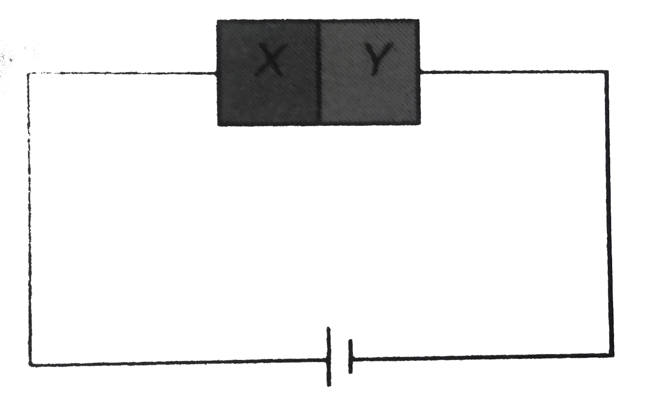
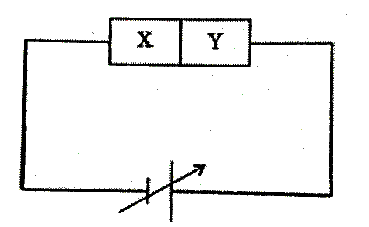
Two semiconductor materials X and Y, shown in the given, are made by doping germanium crystal with indium and arsenic respectively. The two are joined end to end and connected to a battery as shown.
(i) Will the junction be forward biased or reverse biased ?
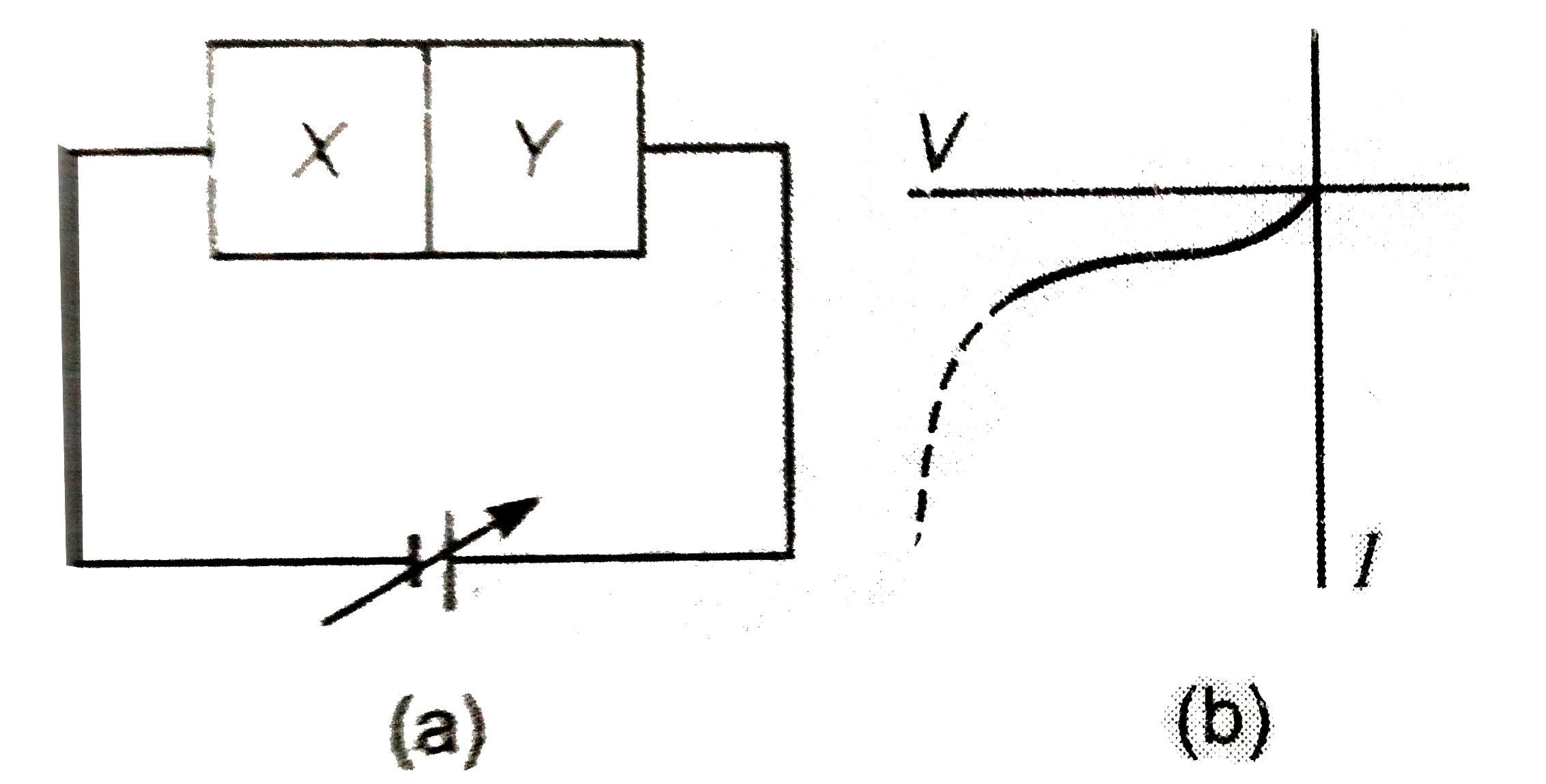
(i) Sketch a V-I graph for this arrangement.
(i) The semiconduct or material X is behaving as p-type, because here the dopant indium is trivalent. Material Y behaves as n-type because there the dopant arsenic is pentavalent. As p-side of junction has been connected to positive terminal of battery, the junction is forward biased.
(i) V-Igraph is shown in

Topper's Solved these Questions
- SEMICONDUCTOR ELECTRONICS : MATERIALS, DEVICES AND SIMPLE CIRCUITSBOOK - U-LIKE SERIESCHAPTER - SEMICONDUCTOR ELECTRONICS : MATERIALS, DEVICES AND SIMPLE CIRCUITSEXERCISE - LONG ANSWER QUESTIONS-I
22 Videos
- SEMICONDUCTOR ELECTRONICS : MATERIALS, DEVICES AND SIMPLE CIRCUITSBOOK - U-LIKE SERIESCHAPTER - SEMICONDUCTOR ELECTRONICS : MATERIALS, DEVICES AND SIMPLE CIRCUITSEXERCISE - SELF ASSESSMENT TEST (MULTIPE CHOICE QUESTIONS )SECTION A
3 Videos
- SEMICONDUCTOR ELECTRONICS : MATERIALS, DEVICES AND SIMPLE CIRCUITSBOOK - U-LIKE SERIESCHAPTER - SEMICONDUCTOR ELECTRONICS : MATERIALS, DEVICES AND SIMPLE CIRCUITSEXERCISE - VERY SHORT ANSWER QUESTIONS
33 Videos
- RAY OPTICS AND OPTICAL INSTRUMENTSBOOK - U-LIKE SERIESCHAPTER - RAY OPTICS AND OPTICAL INSTRUMENTSEXERCISE - SELF ASSESSMENT TEST (SECTION B)
3 Videos
- WAVE OPTICSBOOK - U-LIKE SERIESCHAPTER - WAVE OPTICSEXERCISE - SELF ASSESSMENT TEST SECTION C (VERY SHORT ANSWER QUESTIONS)
4 Videos
Similar Questions
What is an intrinsic semiconductor ? How can this material be converted into (i) p-type, (ii) n-type extrinsic semiconductor? Explain with the help of energy band diagrams.
View SolutionThe temperature coefficient of resistivity of a semiconductor is
View SolutionCarbon and silicon both have four valence electrons each. How then are they distinguished ?
View SolutionA beam of light converges at aoint P. Now a convex lens is placed in the path of the convergent beam at 15 cm from P. At what point does a beam converge if the convex lens has a focal length 10 cm?
View Solution(a) Explain how an unpolarised light gets polarised when incident on the interface separating the two transparent media.
(b) Green light is incident at the polarising angle on a certain transparent medium. The angle of refraction is 30∘. Find
(i) Polarising angle, and
(ii) refractive index of the medium.
View SolutionA semiconductor X is made by dopping a germanium crystal with arsenic (Z=33). A scond semiconductor Y is made by dopping germanium with indium (Z=49). The two are joined end to end and connected to a battery as shown. Which of the following statements is correct?

View SolutionIn a normal operation of a transistor,
(i) base-emitter junction is forward-biased
(ii) base-collector junction is forward-biased
(iii) base-emitter junction is reverse-baised
(iv) base-collector junction is reverse-biased
View Solution
Two semiconductor materials X and Y shown in the given figure, are made by doping germanium crystal with indum and arsenic respectively. The two are joined end to end and connected to a battery as shown.
(i). Will the junction be forward biased or reverse biased.?
(ii). Sketch a V-I graph for this arrangement.
View SolutionWhat happens to the width of depletion layer of a p-n junction when it is (i) forward biased, (ii) reverse biased?
View Solutionशुद्ध जर्मेनियम क्रिस्टल को क्रमशः इंडियन तथा आर्सेनिक से मादित कर दो अर्द्धचालक X और Y बनाये गये हैं

(i ) X - Y सन्धि अग्र अभिनत है अथवा उत्क्रम अभिनत ?
(ii ) इस संयोजन का V - I ग्राफ खींचिये।
View SolutionA junction diode has a resistance of 25 Omega when forward biased and 2500 Omega when reverse biased. What is the current in the diode, for the arrangement shown ?
View SolutionTwo sides of a semiconductor germanuim crystal A and B are doped with arsenic and indium, respectively, They are connected to a battery as shown in figure. The correct graph between current and voltage for the arrangement is
View SolutionA semiconductor material x is made by doping a germanium crystal with indium another semiconductor material y is made by doping a x nad y ar then joined together and connected to a battery will the jucntion be forward or reverse biased also draw the V-I characteristics for the circuit
View SolutionWhat happens to the width of depletion layer of a p-n junction when it is () forward biased, (i) reverse biased ?
View SolutionIn the given diagram [Fig. 14.171, is the junction diode forward biased or reverse biased ?
View Solution
